


MCF51QE128 MCU Series Reference Manual, Rev. 3
Freescale Semiconductor 97
Get the latest version from freescale.com
Chapter 5 Resets, Interrupts, and General System Control
5.5.2 LVD Reset Operation
The LVD can be configured to generate a reset upon detection of a low voltage condition by setting
LVDRE to 1. The low voltage detection threshold is determined by the LVDV bit. After an LVD reset has
occurred, the LVD system holds the MCU in reset until the supply voltage has risen above the low voltage
detection threshold. SRS[LVD] is set following an LVD reset or POR.
5.5.3 LVD Interrupt Operation
When a low voltage condition is detected and the LVD circuit is configured using SPMSC1 for interrupt
operation (LVDE set, LVDIE set, and LVDRE clear), SPMSC1[LVDF] is set and an LVD interrupt request
occurs. The LVDF bit is cleared by writing a 1 to the LVDACK bit in SPMSC1.
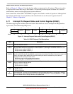
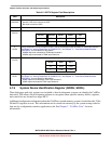
5.5.4 Low-Voltage Warning (LVW) Interrupt Operation
The LVD system has a low voltage warning flag (LVWF) to indicate the supply voltage is approaching,
but is above, the LVD voltage. The LVW also has an interrupt associated with it, enabled by setting the
SPMSC3[LVWIE] bit. If enabled, an LVW interrupt request occurs when the LVWF is set. LVWF is
cleared by writing a 1 to the SPMSC3[LVWACK] bit. There are two user-selectable trip voltages for the
LVW, one high (V
LVWH
) and one low (V
LVWL
). The trip voltage is selected by SPMSC3[LVWV] bit.
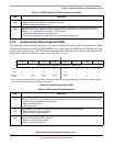
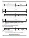
5.6 Peripheral Clock Gating
The MCF51QE128/64/32 includes a clock gating system to manage the bus clock sources to the individual
peripherals. Using this system, you can enable or disable the bus clock to each of the peripherals at the
clock source, eliminating unnecessary clocks to peripherals which are not in use. This reduces the overall
run and wait mode currents.
Out of reset, all peripheral clocks are enabled. For lowest possible run or wait currents, software should
disable the clock source to any peripheral not in use. The actual clock is enabled or disabled immediately
following the write to the clock gating control registers (SCGC1, SCGC2). Any peripheral with a gated
clock cannot be used unless its clock is enabled. Writing to the registers of a peripheral with a disabled
clock has no effect.
NOTE
Software should disable the peripheral before disabling the clocks to the
peripheral. After clocks are re-enabled to a peripheral, the peripheral
registers need to be re-initialized by software.
In stop modes, the bus clock is disabled for all gated peripherals, regardless of the settings in the SCGC1
and SCGC2 registers.
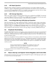
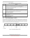
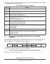
5.7 Reset, Interrupt, and System Control Registers and Control Bits
One 8-bit register in the direct page register space and eight 8-bit registers in the high-page register space
are related to reset and interrupt systems.