


MCF51QE128 MCU Series Reference Manual, Rev. 3
Freescale Semiconductor 37
Get the latest version from freescale.com
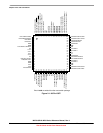
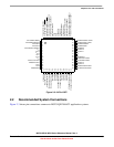
Chapter 2 Pins and Connections
2.2.1 Power
V
DD
and V
SS
are the primary power supply pins for the MCU. This voltage source supplies power to all
I/O buffer circuitry and to an internal voltage regulator. The internal voltage regulator provides regulated
lower-voltage source to the CPU and other internal circuitry of the MCU.
Typically, application systems have two separate capacitors across the power pins. In this case, there
should be a bulk electrolytic capacitor, such as a 10μF tantalum capacitor, to provide bulk charge storage
for the overall system and a 0.1μF ceramic bypass capacitor located as close to the MCU power pins as
practical to suppress high-frequency noise. The MCF51QE128/64/32has two V
DD
pins. Each pin must
have a bypass capacitor for best noise suppression.
V
DDAD
and V
SSAD
are the analog power supply pins for the MCU. This voltage source supplies power to
the ADC module. A 0.1μF ceramic bypass capacitor should be located as close to the MCU power pins as
practical to suppress high-frequency noise.
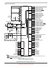
2.2.2 Oscillator
Immediately after reset, the MCU uses an internally generated clock provided by the internal clock source
(ICS) module. For more information on the ICS, see Chapter 12, “Internal Clock Source (S08ICSV3)”.
The oscillator (XOSC) in this MCU is a Pierce oscillator that can accommodate a crystal or ceramic
resonator. Optionally, an external clock source can be connected to the EXTAL input pin.
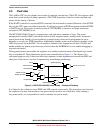
Refer to Figure 2-3 for the following discussion. R
S
(when used) and R
F
should be low-inductance
resistors such as carbon composition resistors. Wire-wound resistors, and some metal film resistors, have
too much inductance. C1 and C2 normally should be high-quality ceramic capacitors specifically designed
for high-frequency applications.
R
F
is used to provide a bias path to keep the EXTAL input in its linear range during crystal startup; its value
is not generally critical. Typical systems use 1 MΩ to 10 MΩ . Higher values are sensitive to humidity and
lower values reduce gain and (in extreme cases) could prevent startup.
C1 and C2 are typically in the 5pF to 25pF range and are chosen to match the requirements of a specific
crystal or resonator. Be sure to take into account printed circuit board (PCB) capacitance and MCU pin
capacitance when selecting C1 and C2. The crystal manufacturer typically specifies a load capacitance that
is the series combination of C1 and C2 (which are usually the same size). As a first-order approximation,
use 10pF as an estimate of combined pin and PCB capacitance for each oscillator pin (EXTAL and XTAL).
2.2.3 RESET and RSTO
After a power-on reset (POR), the PTA5/IRQ/TPM1CLK/RESET pin defaults to a general-purpose input
port pin, PTA5. Setting RSTPE in SOPT1 configures the pin to be the RESET
pin. After configured as
RESET, the pin remains RESET until the next POR. The RESET pin can be used to reset the MCU from
an external source when the pin is driven low. When enabled as the RESET
pin (RSTPE = 1), the pin is
configured as an input with an internal pullup device automatically enabled.