


MCF51QE128 MCU Series Reference Manual, Rev. 3
Freescale Semiconductor 197
Get the latest version from freescale.com
Chapter 9 Rapid GPIO (RGPIO)
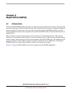
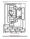
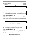
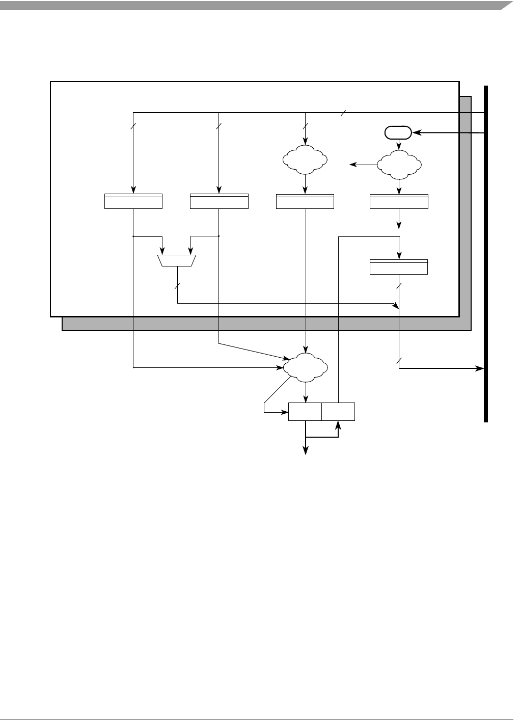
A simplified block diagram of the RGPIO module is shown in Figure 9-3. The details of the pin muxing
and pad logic are device-specific.
Figure 9-3. RGPIO Block Diagram
9.1.2 Features
The major features of the RGPIO module providing 16 bits of high-speed general-purpose input/output are
summarized below:
• Small memory-mapped device connected to the processor’s local bus
— All memory references complete in a single cycle to provide zero wait-state responses
— Located in processor’s high-speed clock domain
• Simple programming model
— Four 16-bit registers, mapped as three program-visible locations
– Register for pin enables
– Register for controlling the pin data direction
– Register for storing output pin data
decode
mux
31
31
0
31
31 15
16
16
0
31
16
15
0
0
rgpio_enable rgpio_direction
rgpio_data_out
rgpio_data_in
Control
Pin Muxing + Pad Logic
RGPIO
module
RGPIO_DATA[15:0]
data from module
data to module
address
On-platform Bus
DirectionPin Enables Write D
ata
Read D
ata