


Chapter 18 Version 1 ColdFire Debug (CF1_DEBUG)
MCF51QE128 MCU Series Reference Manual, Rev. 3
Freescale Semiconductor 361
Get the latest version from freescale.com
NOTE
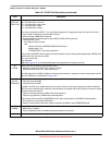
Debug control registers can be written by the external development system
or the CPU through the WDEBUG instruction. These control registers are
write-only from the programming model and they can be written through the
BDM port using the WRITE_DREG command. In addition, the four
configuration/status registers (CSR, XCSR, CSR2, CSR3) can be read
through the BDM port using the READ_DREG command.
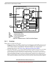
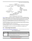
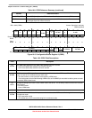
The ColdFire debug architecture supports a number of hardware breakpoint registers that can be
configured into single- or double-level triggers based on the PC or operand address ranges with an optional
inclusion of specific data values. The triggers can be configured to halt the processor or generate a debug
interrupt exception. Additionally, these same breakpoint registers can be used to specify start/stop
conditions for recording in the PST trace buffer.
The core includes four PC breakpoint triggers and a set of operand address breakpoint triggers with two
independent address registers (to allow specification of a range) and an optional data breakpoint with
masking capabilities. Core breakpoint triggers are accessible through the serial BDM interface or written
through the supervisor programming model using the WDEBUG instruction.
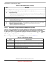
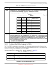
18.3.1 Configuration/Status Register (CSR)
CSR defines the debug configuration for the processor and memory subsystem and contains status
information from the breakpoint logic. CSR is accessible from the programming model using the
WDEBUG instruction and through the BDM port using the READ_DREG and WRITE_DREG
commands.
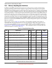
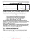
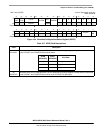
0x18 PC breakpoint register 1 (PBR1) 32 W PBR1[0] = 0 18.3.8/18-376
0x1A PC breakpoint register 2 (PBR2) 32 W PBR2[0] = 0 18.3.8/18-376
0x1B PC breakpoint register 3 (PBR3) 32 W PBR3[0] = 0 18.3.8/18-376
0x20 + n;
n = 0–11
PST Trace Buffer n (PSTBn); n =0–11 32 R (BDM)
3
Undefined,
Unaffected
18.4.3.2/18-413
1
The most significant byte of the XCSR, CSR2 and CSR3 registers supports special control functions and are writeable via BDM
using the WRITE_XCSR_BYTE, WRITE_CSR2_BYTE, and WRITE_CXSR3_BYTE commands. They can be read from BDM
using the READ_XCSR_BYTE, READ_CSR2_BYTE, and READ_CSR3_BYTE commands. These 3 registers, along with the
CSR, can also be referenced as 32-bit quantities using the BDM READ_DREG and WRITE_DREG commands.
2
Each debug register is accessed as a 32-bit value; undefined fields are reserved and must be cleared.
3
The contents of the PST trace buffer is read from BDM (32 bits per access) using READ_PSTB commands.
Table 18-4. Debug Module Memory Map (continued)
DRc Register Name
Width
(bits)
Access Reset Value
Section/
Page