


MCF51QE128 MCU Series Reference Manual, Rev. 3
128 Freescale Semiconductor
Get the latest version from freescale.com
Chapter 6 Parallel Input/Output Control
6.7.4.4 Port D Slew Rate Enable Register (PTDSE)
6.7.4.5 Port D Drive Strength Selection Register (PTDDS)
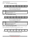
6.7.5 Port E Registers
Port E is controlled by the registers listed below.
6.7.5.1 Port E Data Register (PTED)
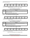
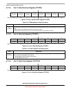
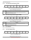
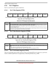
76543210
R
PTDSE7 PTDSE6 PTDSE5 PTDSE4 PTDSE3 PTDSE2 PTDSE1 PTDSE0
W
Reset:00000000
Figure 6-25. Slew Rate Enable for Port D Register (PTDSE)
Table 6-22. PTDSE Register Field Descriptions
Field Description
7–0
PTDSEn
Output Slew Rate Enable for Port D Bits. Each of these control bits determines if the output slew rate control is
enabled for the associated PTD pin. For port D pins configured as inputs, these bits have no effect.
0 Output slew rate control disabled for port D bit n.
1 Output slew rate control enabled for port D bit n.
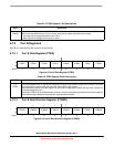
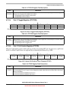
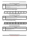
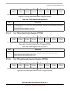
76543210
R
PTDDS7 PTDDS6 PTDDS5 PTDDS4 PTDDS3 PTDDS2 PTDDS1 PTDDS0
W
Reset:00000000
Figure 6-26. Drive Strength Selection for Port D Register (PTDDS)
Table 6-23. PTDDS Register Field Descriptions
Field Description
7–0
PTDDSn
Output Drive Strength Selection for Port D Bits. Each of these control bits selects between low and high output
drive for the associated PTD pin. For port D pins configured as inputs, these bits have no effect.
0 Low output drive strength selected for port D bit n.
1 High output drive strength selected for port D bit n.
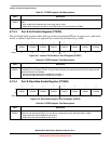
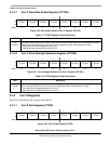
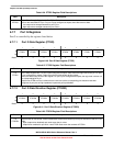
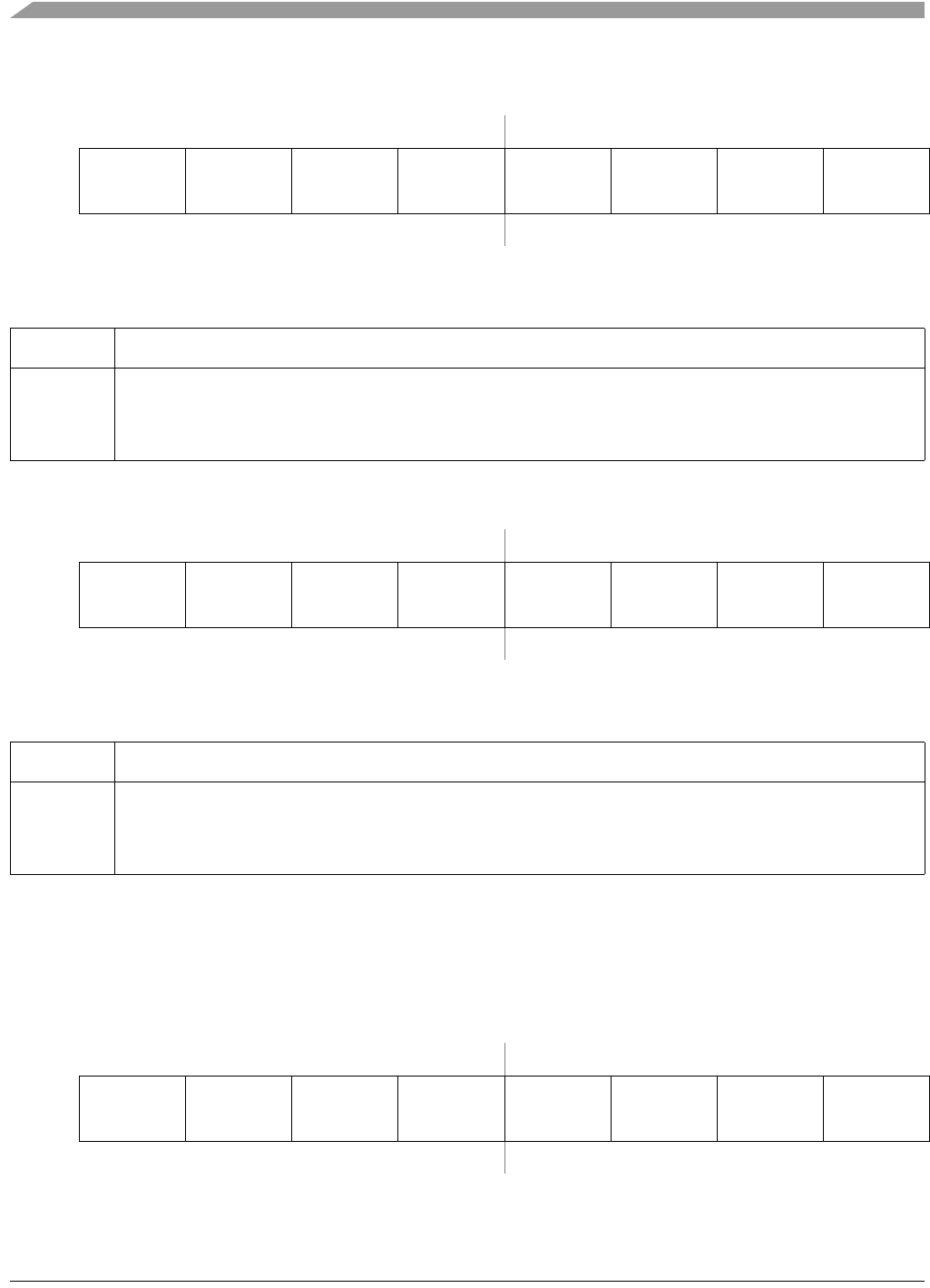
76543210
R
PTED7 PTED6 PTED5 PTED4 PTED3 PTED2 PTED1 PTED0
W
Reset:00000000
Figure 6-27. Port E Data Register (PTED)