


MCF51QE128 MCU Series Reference Manual, Rev. 3
Freescale Semiconductor 319
Get the latest version from freescale.com
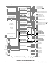
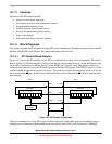
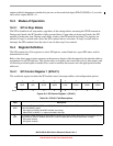
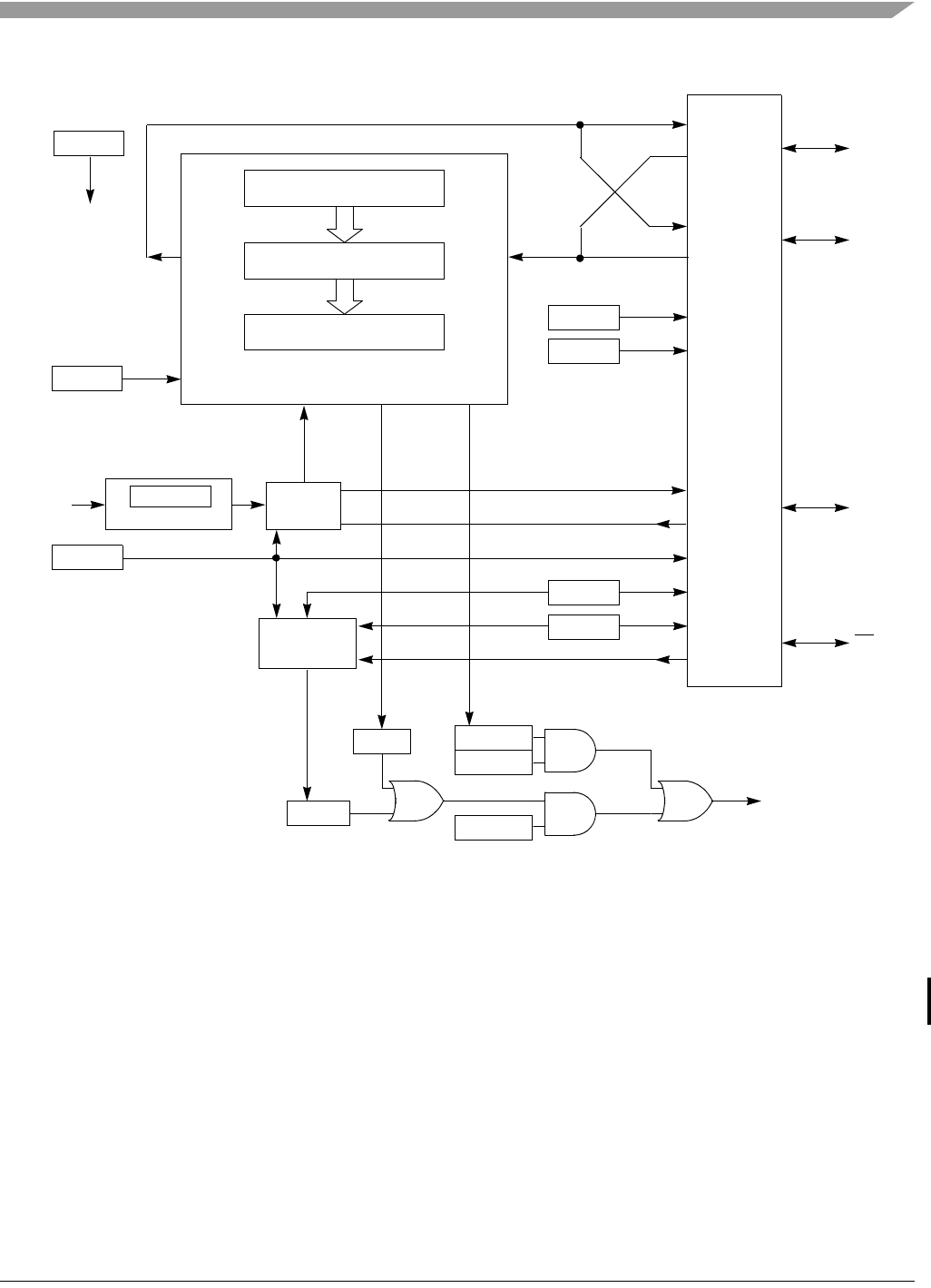
Figure 16-3. SPI Module Block Diagram
16.1.5 SPI Baud Rate Generation
As shown in Figure 16-4, the clock source for the SPI baud rate generator is the bus clock. The three
prescale bits (SPIxBR[SPPR]) choose a prescale divisor of 1, 2, 3, 4, 5, 6, 7, or 8. The three rate select bits
(SPIxBR[SPR]) divide the output of the prescaler stage by 2, 4, 8, 16, 32, 64, 128, or 256 to obtain the
internal SPI master mode bit-rate clock.
SPI Shift Register
Shift
Clock
Shift
Direction
Rx Buffer
Full
Tx Buffer
Empty
Shift
Out
Shift
In
Enable
SPI System
Clock
Logic
Clock Generator
Bus Rate
Clock
Master/Slave
Mode Select
Mode Fault
Detection
Master Clock
Slave Clock
SPI
Interrupt
Request
Pin Control
M
S
Master/
Slave
MOSI
(MOMI)
MISO
(SISO)
SPSCK
SS
M
S
S
M
MODF
SPE
LSBFE
MSTR
SPRF
SPTEF
SPTIE
SPIE
MODFEN
SSOE
SPC0
BIDIRO
SPIxBR
Tx Buffer (Write SPIxD)
Rx Buffer (Read SPIxD)