


MCF51QE128 MCU Series Reference Manual, Rev. 3
118 Freescale Semiconductor
Get the latest version from freescale.com
Chapter 6 Parallel Input/Output Control
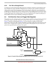
6.5.4 Keyboard Interrupt Initialization
When an interrupt pin is first enabled, it is possible to get a false interrupt flag. To prevent a false interrupt
request during pin interrupt initialization, do the following:
1. Mask interrupts by clearing KBIxSC[KBIE].
2. Select the pin polarity by setting the appropriate KBIxES[KBEDGn] bits.
3. If using internal pull-up/pull-down device, configure the associated pull enable bits in KBIxPE.
4. Enable the interrupt pins by setting the appropriate KBIxPE[KBIPEn] bits.
5. Write to KBIxSC[KBACK] to clear any false interrupts.
6. Set KBIxSC[KBIE] to enable interrupts.
6.6 Pin Behavior in Stop Modes
Pin behavior following execution of a STOP instruction depends on the entered stop mode. An explanation
of pin behavior for the various stop modes follows:
• Stop2 mode is a partial power-down mode, whereby I/O latches are maintained in their state as
before the STOP instruction was executed (port states are lost and need to be restored upon exiting
stop2). CPU register status and the state of I/O registers should be saved in RAM before the STOP
instruction is executed to place the MCU in stop2 mode.
Upon recovery from stop2 mode, before accessing any I/O, examine the state of the
SPMSC2[PPDF] bit. If the PPDF bit is cleared, I/O must be initialized as if a power-on-reset had
occurred. If the PPDF bit is set, I/O register states should be restored from the values saved in RAM
before the STOP instruction was executed and peripherals may require initialization or restoration
to their pre-stop condition. Then, write a 1 to the SPMSC2[PPDACK] bit. Access to I/O is now
permitted again in the user application program.
• In stop3 and stop4 modes, all I/O is maintained because internal logic circuity stays powered. Upon
recovery, normal I/O function is available to the user.
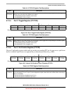
6.7 Parallel I/O, Keyboard Interrupt, and Pin Control Registers
This section provides information about the registers associated with the parallel I/O ports. The data, data
direction registers, and keyboard interrupt registers are located in page zero of the memory map. The
pull-up, slew rate, drive strength, and interrupt control registers are located in the high page section of the
memory map.
Refer to tables in Chapter 4, “Memory,” for the absolute address assignments for all parallel I/O and their
pin control registers. This section refers to registers and control bits only by their names. A Freescale
Semiconductor-provided equate or header file normally is translates these names into the appropriate
absolute addresses.
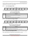
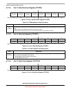
6.7.1 Port A Registers
Port A is controlled by the registers listed below.