


Chapter 18 Version 1 ColdFire Debug (CF1_DEBUG)
MCF51QE128 MCU Series Reference Manual, Rev. 3
360 Freescale Semiconductor
Get the latest version from freescale.com
18.3 Memory Map/Register Definition
In addition to the BDM commands that provide access to the processor’s registers and the memory
subsystem, the debug module contains a number of registers. Most of these registers (all except the
PST/DDATA trace buffer) are also accessible (write-only) from the processor’s supervisor programming
model by executing the WDEBUG instruction. Thus, the breakpoint hardware in the debug module can be
read (certain registers) or written by the external development system using the serial debug interface or
written by the operating system running on the processor core. Software is responsible for guaranteeing
that accesses to these resources are serialized and logically consistent. The hardware provides a locking
mechanism in the CSR to allow the external development system to disable any attempted writes by the
processor to the breakpoint registers (setting CSR[IPW]). BDM commands must not be issued during the
processor’s execution of the WDEBUG instruction to configure debug module registers or the resulting
behavior is undefined.
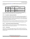
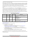
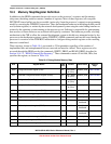
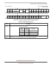
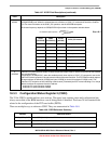
These registers, shown in Table 18-4, are treated as 32-bit quantities regardless of the number of
implemented bits and unimplemented bits are reserved and must be cleared. These registers are also
accessed through the BDM port by the commands, WRITE_DREG and READ_DREG, described in
Section 18.4.1.5, “BDM Command Set Summary.” These commands contain a 5-bit field, DRc, that
specifies the register, as shown in Table 18-4.
Table 18-4. Debug Module Memory Map
DRc Register Name
Width
(bits)
Access Reset Value
Section/
Page
0x00 Configuration/status register (CSR) 32 R/W (BDM),
W (CPU)
0x0090_0000 18.3.1/18-361
0x01 Extended Configuration/Status Register (XCSR) 32 R/W
1
(BDM),
W (CPU)
0x0000_0000 18.3.2/18-364
0x02 Configuration/Status Register 2 (CSR2) 32 R/W
1
(BDM),
W (CPU)
See Section 18.3.3/18-367
0x03 Configuration/Status Register 3 (CSR3) 32
2
R/W
1
(BDM),
W (CPU)
0x0000_0000 18.3.4/18-370
0x05 BDM address attribute register (BAAR) 32
2
W 0x0000_0005 18.3.5/18-371
0x06 Address attribute trigger register (AATR) 32
2
W 0x0000_0005 18.3.6/18-372
0x07 Trigger definition register (TDR) 32 W 0x0000_0000 18.3.7/18-373
0x08 PC breakpoint register 0 (PBR0) 32 W Undefined,
Unaffected
18.3.8/18-376
0x09 PC breakpoint mask register (PBMR) 32 W Undefined,
Unaffected
18.3.8/18-376
0x0C Address breakpoint high register (ABHR) 32 W Undefined,
Unaffected
18.3.9/18-378
0x0D Address breakpoint low register (ABLR) 32 W 0x0000_0000 18.3.9/18-378
0x0E Data breakpoint register (DBR) 32 W 0x0000_0000 18.3.10/18-379
0x0F Data breakpoint mask register (DBMR) 32 W 0x0000_0000 18.3.10/18-379