


MCF51QE128 MCU Series Reference Manual, Rev. 3
72 Freescale Semiconductor
Get the latest version from freescale.com
Chapter 4 Memory
• Command interface for fast program and erase operation
• Up to 100,000 program/erase cycles at typical voltage and temperature
• Flexible block protection (on any 2-Kbyte memory boundary)
• Security feature to prevent unauthorized access to on-chip memory and resources
• Auto power-down for low-frequency read accesses
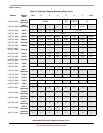
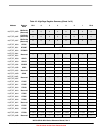
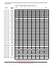
4.4.2 Register Descriptions
The flash module contains a set of 16 control and status registers located between 0x(00)00_0000 and
0x(00)00_000F. Detailed descriptions of each register bit are provided in the following sections.
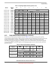
4.4.2.1 Flash Clock Divider Register (FCDIV)
The FCDIV register controls the length of timed events in program and erase algorithms executed by the
flash memory controller. All bits in the FCDIV register are readable and writable with restrictions as
determined by the value of FDIVLD when writing to the FCDIV register.
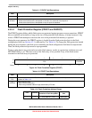
4.4.2.2 Flash Options Register (FOPT and NVOPT)
The FOPT register holds all bits associated with the security of the MCU and flash module. All bits in the
FOPT register are readable but are not writable.
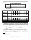
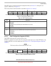
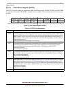
76543210
R
FDIVLD PRDIV8 FDIV
W
Reset00000000
Figure 4-3. Flash Clock Divider Register (FCDIV)
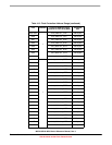
Table 4-9. FCDIV Field Descriptions
Field Description
7
FDIVLD
Clock Divider Load Control. When writing to the FCDIV register for the first time after a reset, the value of the
FDIVLD bit written controls the future ability to write to the FCDIV register:
0 Writing a 0 to FDIVLD locks the FCDIV register contents; all future writes to FCDIV are ignored.
1 Writing a 1 to FDIVLD keeps the FCDIV register writable; next write to FCDIV is allowed.
When reading the FCDIV register, the value of the FDIVLD bit read indicates the following:
0 FCDIV register has not been written to since the last reset.
1 FCDIV register has been written to since the last reset.
6
PRDIV8
Enable Prescalar by 8
.
0 The bus clock is directly fed into the clock divider.
1 The bus clock is divided by 8 before feeding into the clock divider.
5–0
FDIV
Clock Divider Bits. The combination of PRDIV8 and FDIV[5:0] must divide the bus clock down to a frequency
of 150 kHz–200 kHz. The minimum divide ratio is 2 (PRDIV8=0, FDIV=0x01) and the maximum divide ratio is
512 (PRDIV8=1, FDIV=0x3F). Refer to Section 4.5.1.1, “Writing the FCDIV Register” for more information.