


MCF51QE128 MCU Series Reference Manual, Rev. 3
Freescale Semiconductor 307
Get the latest version from freescale.com
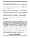
15.3.3 Receiver Functional Description
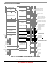
In this section, the receiver block diagram (Figure 15-4) is a guide for the overall receiver functional
description. Next, the data sampling technique used to reconstruct receiver data is described in more detail.
Finally, two variations of the receiver wakeup function are explained.
The receiver input is inverted by setting RXINV. The receiver is enabled by setting the RE bit in SCIxC2.
Character frames consist of a start bit of logic 0, eight (or nine) data bits (lsb first), and a stop bit of logic
1. For information about 9-bit data mode, refer to Section 15.3.5.1, “8- and 9-Bit Data Modes”. For the
remainder of this discussion, assume the SCI is configured for normal 8-bit data mode.
After receiving the stop bit into the receive shifter, and provided the receive data register is not already
full, the data character is transferred to the receive data register and the receive data register full (RDRF)
status flag is set. If RDRF was already set indicating the receive data register (buffer) was already full, the
overrun (OR) status flag is set and the new data is lost. Because the SCI receiver is double-buffered, the
program has one full character time after RDRF is set before the data in the receive data buffer must be
read to avoid a receiver overrun.
When a program detects that the receive data register is full (RDRF = 1), it gets the data from the receive
data register by reading SCIxD. The RDRF flag is cleared automatically by a two-step sequence normally
satisfied in the course of the user’s program that manages receive data. Refer to Section 15.3.4, “Interrupts
and Status Flags,” for more details about flag clearing.
15.3.3.1 Data Sampling Technique
The SCI receiver uses a 16× baud rate clock for sampling. The receiver starts by taking logic level samples
at 16 times the baud rate to search for a falling edge on the RxD serial data input pin. A falling edge is
defined as a logic 0 sample after three consecutive logic 1 samples. The 16× baud rate clock divides the
bit time into 16 segments labeled RT1 through RT16. When a falling edge is located, three more samples
are taken at RT3, RT5, and RT7 to make sure this was a real start bit and not merely noise. If at least two
of these three samples are 0, the receiver assumes it is synchronized to a receive character.
The receiver then samples each bit time, including the start and stop bits, at RT8, RT9, and RT10 to
determine the logic level for that bit. The logic level is interpreted to be that of the majority of the samples
taken during the bit time. In the case of the start bit, the bit is assumed to be 0 if at least two of the samples
at RT3, RT5, and RT7 are 0 even if one or all of the samples taken at RT8, RT9, and RT10 are 1s. If any
sample in any bit time (including the start and stop bits) in a character frame fails to agree with the logic
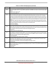
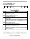
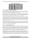
Table 15-8. Break Character Length
BRK13 M Break Character Length
0 0 10 bit times
0 1 11 bit times
1 0 13 bit times
1 1 14 bit times