


MCF51QE128 MCU Series Reference Manual, Rev. 3
Freescale Semiconductor 299
Get the latest version from freescale.com
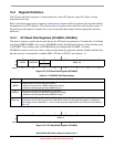
15.2.2 SCI Control Register 1 (SCIxC1)
This read/write register controls various optional features of the SCI system.
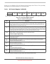
Table 15-2. SCIxBDL Field Descriptions
Field Description
7–0
SBR[7:0]
Baud Rate Modulo Divisor. These 13 bits in SBR[12:0] are referred to collectively as BR, and they set the modulo
divide rate for the SCI baud rate generator. When BR is cleared, the SCI baud rate generator is disabled to
reduce supply current. When BR is 1 – 8191, the SCI baud rate equals BUSCLK/(16×BR). See also BR bits in
Ta bl e 1 5- 1.
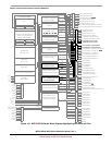
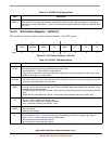
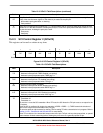
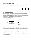
76543210
R
LOOPS SCISWAI RSRC M WAKE ILT PE PT
W
Reset00000000
Figure 15-7. SCI Control Register 1 (SCIxC1)
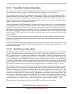
Table 15-3. SCIxC1 Field Descriptions
Field Description
7
LOOPS
Loop Mode Select. Selects between loop back modes and normal 2-pin full-duplex modes. When LOOPS is set,
the transmitter output is internally connected to the receiver input.
0 Normal operation — RxD and TxD use separate pins.
1 Loop mode or single-wire mode where transmitter outputs are internally connected to receiver input. (See
RSRC bit.) RxD pin is not used by SCI.
6
SCISWAI
SCI Stops in Wait Mode
0 SCI clocks continue to run in wait mode so the SCI can be the source of an interrupt that wakes up the CPU.
1 SCI clocks freeze while CPU is in wait mode.
5
RSRC
Receiver Source Select. This bit has no meaning or effect unless the LOOPS bit is set to 1. When LOOPS is set,
the receiver input is internally connected to the TxD pin and RSRC determines whether this connection is also
connected to the transmitter output.
0 Provided LOOPS is set, RSRC is cleared, selects internal loop back mode and the SCI does not use the RxD
pins.
1 Single-wire SCI mode where the TxD pin is connected to the transmitter output and receiver input.
4
M
9-Bit or 8-Bit Mode Select
0 Normal — start + 8 data bits (lsb first) + stop.
1 Receiver and transmitter use 9-bit data characters
start + 8 data bits (lsb first) + 9th data bit + stop.
3
WAKE
Receiver Wakeup Method Select. Refer to Section 15.3.3.2, “Receiver Wakeup Operation” for more information.
0 Idle-line wakeup.
1 Address-mark wakeup.
2
ILT
Idle Line Type Select. Setting this bit to 1 ensures that the stop bit and logic 1 bits at the end of a character do
not count toward the 10 or 11 bit times of logic high level needed by the idle line detection logic. Refer to
Section 15.3.3.2.1, “Idle-Line Wakeup” for more information.
0 Idle character bit count starts after start bit.
1 Idle character bit count starts after stop bit.