


MCF51QE128 MCU Series Reference Manual, Rev. 3
Freescale Semiconductor 27
Get the latest version from freescale.com
Chapter 1 Device Overview
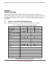
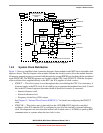
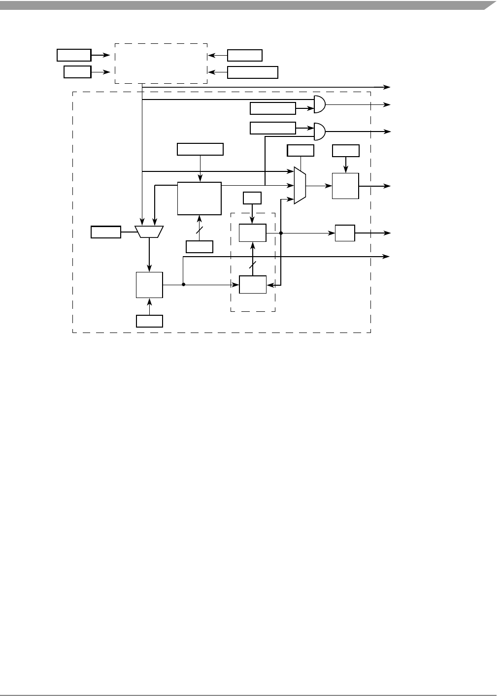
Figure 1-2. Simplified ICS Block Diagram
1.4.2 System Clock Distribution
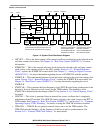
Figure 1-3 shows a simplified clock connection diagram. Some modules in the MCU have selectable clock
inputs as shown. The clock inputs to the modules indicate the clock(s) used to drive the module function.
All memory mapped registers associated with the modules (except RGPIO) are clocked with the peripheral
clock (BUSCLK). The RGPIO registers are clocked with the CPU clock (ICSOUT). With the exception
of the oscillator clock supplied directly to the RTC, the ICS supplies all clock sources:
• ICSOUT — This clock source is used throughout the core including the CPU. For consistency, it
is known simply as the CPU clock. It is divided by two to generate the peripheral bus clock. Control
bits in the ICS control registers determine which of three clock sources is connected:
— Internal reference clock
— External reference clock
— Frequency-locked loop (FLL) output
See Chapter 12, “Internal Clock Source (S08ICSV3),” for details on configuring the ICSOUT
clock.
• ICSLCLK — This clock source is derived from the 10/20 MHz DCO (digitally controlled
oscillator) of the ICS when the ICS is configured to run off of the internal or external reference
clock. Development tools can select this internal self-clocked source (~10 MHz) to speed up BDC
communications in systems where the bus clock is slow.
DCO
Filter
RDIV
TRIM
/ 2
9
External Reference
IREFS
Clock Source
Block
CLKS
n=0-7
/ 2
n
n=0-3
/ 2
n
Internal
Reference
Clock
BDIV
9
ICSLCLK
ICSOUT
ICSIRCLK
EREFS
RANGE
EREFSTEN
HGO
Optional
IREFSTEN
ICSERCLK
Internal Clock Source Block
LP
ICSFFCLK
ERCLKEN
IRCLKEN
DCOOUT
FLL
RDIV_CLK
RTC