


MCF51QE128 MCU Series Reference Manual, Rev. 3
78 Freescale Semiconductor
Get the latest version from freescale.com
Chapter 4 Memory
4. Effects resulting from illegal flash command write sequences or aborting flash operations
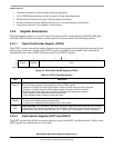
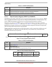
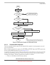
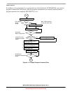
4.5.1.1 Writing the FCDIV Register
Prior to issuing any flash command after a reset, write the FCDIV register to divide the bus clock down to
150–200 kHz. The FCDIV[PRDIV8, FDIV] bits must be set as described in Figure 4-9.
For example, if the bus clock frequency is 25 MHz, FCDIV[FDIV] should be set to 0x0F (001111) and the
FCDIV[PRDIV8] bit set to 1. The resulting FCLK frequency is then 195 kHz. In this case, the flash
program and erase algorithm timings are increased over the optimum target by:
(200 - 195) ÷ 200 = 3% Eqn. 4-1
CAUTION
Program and erase command execution time increase proportionally with
the period of FCLK. Programming or erasing the flash memory with
FCLK less than 150 kHz should be avoided. Setting FCDIV to a value such
that FCLK is less than 150 kHz can destroy the flash memory due to
overstress. Setting FCDIV to a value where FCLK is greater than 200 kHz
can result in incomplete programming or erasure of the flash memory cells.
If the FCDIV register is written, the FDIVLD bit is automatically set. If the FDIVLD bit is 0, the FCDIV
register has not been written since the last reset. If the FCDIV register has not been written to, the flash
command loaded during a command write sequence does not execute and FSTAT[FACCERR] is set.