


MCF51QE128 MCU Series Reference Manual, Rev. 3
198 Freescale Semiconductor
Get the latest version from freescale.com
Chapter 9 Rapid GPIO (RGPIO)
– Register for reading current pin state
– The two data registers (read, write) are mapped to a single program-visible location
— Alternate addresses to perform data set, clear, and toggle functions using simple writes
— Separate read and write programming model views enable simplified driver software
– Support for any access size (byte, word, or longword)
9.1.3 Modes of Operation
The RGPIO module does not support any special modes of operation. As a memory-mapped device
located on the processor’s high-speed local bus, it responds based strictly on memory address and does not
consider the operating mode (supervisor, user) of its references.
9.2 External Signal Description
9.2.1 Overview
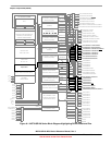
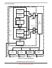
As shown in Figure 9-3, the RGPIO module’s interface to external logic is indirect via the device
pin-muxing and pad logic. For a list of the associated RGPIO input/output signals, see Table 9-1.
9.2.2 Detailed Signal Descriptions
Table 9-2 provides descriptions of the RGPIO module’s input and output signals.
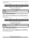
Table 9-1. RGPIO Module External I/O Signals
Signal Name Type Description
RGPIO[15:0] I/O RGPIO Data Input/Output
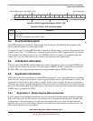
Table 9-2. RGPIO Detailed Signal Descriptions
Signal I/O Description
RGPIO[15:0] I/O Data Input/Output. When configured as an input, the state of this signal is reflected in the read
data register. When configured as an output, this signal is the output of the write data register.
State
Meaning
Asserted—
Input: Indicates the RGPIO pin was sampled as a logic high at the time of
the read.
Output: Indicates a properly-enabled RGPIO output pin is to be driven high.
Negated—
Input: Indicates the RGPIO pin was sampled as a logic low at the time of the
read.
Output: Indicates a properly-enabled RGPIO output pin is to be driven low.
Timing Assertion/Negation—
Input: Anytime. The input signal is sampled at the rising-edge of the
processor’s high-speed clock on the data phase cycle of a read transfer of
this register.
Output: Occurs at the rising-edge of the processor’s high-speed clock on
the data phase cycle of a write transfer to this register. This output is
asynchronously cleared by system reset.