


MCF51QE128 MCU Series Reference Manual, Rev. 3
326 Freescale Semiconductor
Get the latest version from freescale.com
indicate there is room in the buffer to queue another transmit character if desired, and the SPI serial transfer
starts.
During the SPI transfer, data is sampled (read) on the MISO pin at one SPSCK edge and shifted, changing
the bit value on the MOSI pin, one-half SPSCK cycle later. After eight SPSCK cycles, the data that was
in the shift register of the master has been shifted out the MOSI pin to the slave while eight bits of data
were shifted in the MISO pin into the master’s shift register. At the end of this transfer, the received data
byte is moved from the shifter into the receive data buffer and SPRF is set to indicate the data can be read
by reading SPIxD. If another byte of data is waiting in the transmit buffer at the end of a transfer, it is
moved into the shifter, SPTEF is set, and a new transfer is started.
Normally, SPI data is transferred most significant bit (msb) first. If SPIxC1[LSBFE] is set, SPI data is
shifted lsb first.
When the SPI is configured as a slave, its SS pin must be driven low before a transfer starts and SS must
stay low throughout the transfer. If a clock format where CPHA is cleared is selected, SS must be driven
to a logic 1 between successive transfers. If CPHA is set, SS may remain low between successive transfers.
See Section 16.5.1, “SPI Clock Formats,” for more details.
Because the transmitter and receiver are double buffered, a second byte, in addition to the byte currently
being shifted out, can be queued into the transmit data buffer. A previously received character can be in
the receive data buffer while a new character is being shifted in. The SPTEF flag indicates when the
transmit buffer has room for a new character. The SPRF flag indicates when a received character is
available in the receive data buffer. The received character must be read out of the receive buffer (read
SPIxD) before the next transfer is finished or a receive overrun error results.
In the case of a receive overrun, the new data is lost because the receive buffer held the previous character
and was not ready to accept the new data. There is no indication for such an overrun condition so the user
must ensure that previous data has been read from the receive buffer before a new transfer is initiated.
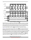
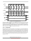
16.5.1 SPI Clock Formats
To accommodate a wide variety of synchronous serial peripherals from different manufacturers, the SPI
system has a clock polarity (CPOL) bit and a clock phase (CPHA) control bit to select one of four clock
formats for data transfers. CPOL selectively inserts an inverter in series with the clock. CPHA chooses
between two different clock phase relationships between the clock and data.
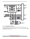
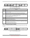
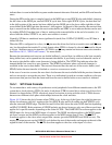
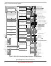
Figure 16-10 shows the clock formats when CPHA is set. At the top of the figure, the eight bit times are
shown for reference with bit 1 starting at the first SPSCK edge and bit 8 ending one-half SPSCK cycle
after the sixteenth SPSCK edge. The msb first and lsb first lines show the order of SPI data bits depending
on SPIxC1[LSBFE]. Both variations of SPSCK polarity are shown; however, only one of these waveforms
applies for a specific transfer, depending on the value in CPOL. The SAMPLE IN waveform applies to the
MOSI input of a slave or the MISO input of a master. The MOSI waveform applies to the MOSI output
pin from a master and the MISO waveform applies to the MISO output from a slave. The SS
OUT
waveform applies to the slave select output from a master (provided MODFEN and SSOE are set). The
master SS
output asserts one-half SPSCK cycle before the start of the transfer and negates at the end of the
eighth bit time of the transfer. The SS
IN waveform applies to the slave select input of a slave.