


MCF51QE128 MCU Series Reference Manual, Rev. 3
Freescale Semiconductor 79
Get the latest version from freescale.com
Chapter 4 Memory
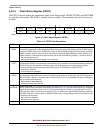
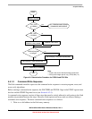
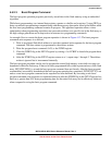
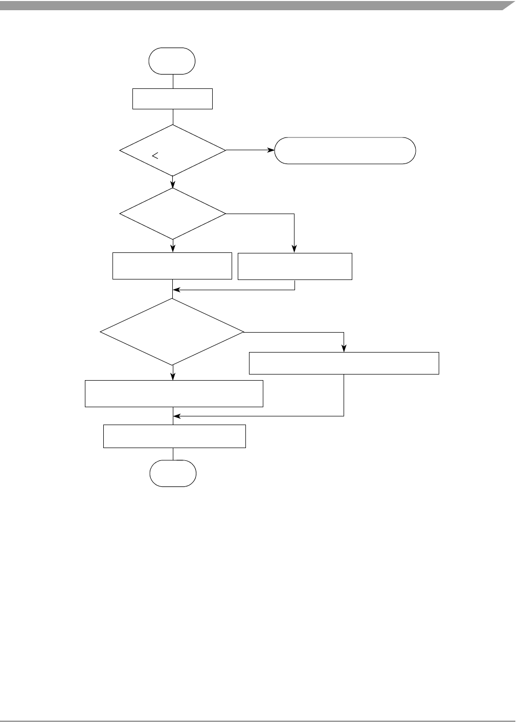
Figure 4-9. Determination Procedure for PRDIV8 and FDIV Bits
4.5.1.2 Command Write Sequence
The flash command controller supervises the command write sequence to execute program, erase, and
erase verify algorithms.
Before starting a command write sequence, the FACCERR and FPVIOL flags in the FSTAT register must
be clear and the FCBEF flag must be set (see Section 4.4.2.5).
A command write sequence consists of three steps that must be strictly adhered to with writes to the flash
module not permitted between the steps. However, flash register and array reads are allowed during a
command write sequence. The basic command write sequence is as follows:
1. Write to a valid address in the flash array memory.
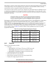
set PRDIV8 = 1
yes
no
PRDIV8 = 0 (reset)
≥ 12.8MHz?
FCLK = (PRDCLK)/(1+FDIV[5:0])
PRDCLK = bus_clock
PRDCLK = bus_clock/8
PRDCLK[kHz]/200
no
set FDIV[5:0] = PRDCLK[kHz]/200-1
yes
START
an integer?
set FDIV[5:0] = INT(PRDCLK[kHz]/200)
END
bus_clock
no
yes
0.3MHz?
bus_clock
ALL PROGRAM AND ERASE
COMMANDS IMPOSSIBLE
Note:
• FCLK is the clock of the flash timing control block
• INT(x) is the integer part of x (e.g. INT(4.323) = 4)