


Chapter 18 Version 1 ColdFire Debug (CF1_DEBUG)
MCF51QE128 MCU Series Reference Manual, Rev. 3
384 Freescale Semiconductor
Get the latest version from freescale.com
When a development system is connected, it can pull BKGD and RESET low, release RESET to select
active background (halt) mode rather than normal operating mode, and then release BKGD. It is not
necessary to reset the target MCU to communicate with it through the background debug interface. There
is also a mechanism to generate a reset event in response to setting CSR2[BDFR].
18.4.1.3 BDM Communication Details
The BDC serial interface requires the external host controller to generate a falling edge on the BKGD pin
to indicate the start of each bit time. The external controller provides this falling edge whether data is
transmitted or received.
BKGD is a pseudo-open-drain pin that can be driven by an external controller or by the MCU. Data is
transferred msb first at 16 BDC clock cycles per bit (nominal speed). The interface times-out if 512 BDC
clock cycles occur between falling edges from the host. If a time-out occurs, the status of any command
in progress must be determined before new commands can be sent from the host. To check the status of
the command, follow the steps detailed in the bit description of XCSR[CSTAT] in Table 18-6.
The custom serial protocol requires the debug pod to know the target BDC communication clock speed.
The clock switch (CLKSW) control bit in the XCSR[31–24] register allows you to select the BDC clock
source. The BDC clock source can either be the bus clock or the alternate BDC clock source. When the
MCU is reset in normal user mode, CLKSW is cleared and that selects the alternate clock source. This
clock source is a fixed frequency independent of the bus frequency so it does change if the user modifies
clock generator settings. This is the preferred clock source for general debugging.
When the MCU is reset in active background (halt) mode, CLKSW is set which selects the bus clock as
the source of the BDC clock. This CLKSW setting is most commonly used during flash memory
programming because the bus clock can usually be configured to operate at the highest allowed bus
frequency to ensure the fastest possible flash programming times. Since the host system is in control of
changes to clock generator settings, it knows when a different BDC communication speed should be used.
The host programmer also knows that no unexpected change in bus frequency could occur to disrupt BDC
communications.
Normally, setting CLKSW should not be used for general debugging because there is no way to ensure the
application program does not change the clock generator settings. This is especially true in the case of
application programs that are not yet fully debugged.
After any reset (or at any other time), the host system can issue a SYNC command to determine the speed
of the BDC clock. CLKSW may be written using the serial WRITE_XCSR_BYTE command through the
BDC interface. CLKSW is located in the special XCSR byte register in the BDC module and it is not
accessible in the normal memory map of the ColdFire core. This means that no program running on the
processor can modify this register (intentionally or unintentionally).
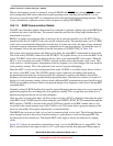
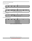
The BKGD pin can receive a high- or low-level or transmit a high- or low-level. The following diagrams
show timing for each of these cases. Interface timing is synchronous to clocks in the target BDC, but
asynchronous to the external host. The internal BDC clock signal is shown for reference in counting
cycles.
Figure 18-15 shows an external host transmitting a logic 1 or 0 to the BKGD pin of a target MCU. The
host is asynchronous to the target so there is a 0–1 cycle delay from the host-generated falling edge to