


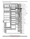


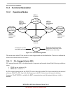

Internal Clock Source (S08ICSV3)
MCF51QE128 MCU Series Reference Manual, Rev. 3
252 Freescale Semiconductor
Get the latest version from freescale.com
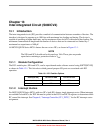
12.3.4 ICS Status and Control (ICSSC)
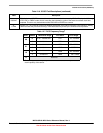
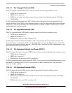
Table 12-5. ICSTRM Field Descriptions
Field Description
7:0
TRIM
ICS Trim Setting. The TRIM bits control the internal reference clock frequency by controlling the internal
reference clock period. The bits’ affects are binary weighted (bit 1 adjusts twice as much as bit 0). Increasing the
binary value in TRIM increases the period and decreasing the value decreases the period.
An additional fine trim bit is available in ICSSC as the FTRIM bit.
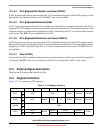
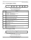
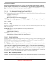
76543210
R DRST
DMX32
IREFST CLKST OSCINIT
FTRIM
1
1
FTRIM is loaded during reset from a factory programmed location when not in any BDM mode. If in a BDM mode,
FTRIM gets loaded with a value of 1’b0.
WDRS
Reset:0001000
Figure 12-6. ICS Status and Control Register (ICSSC)
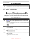
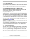
Table 12-6. ICSSC Field Descriptions
Field Description
7-6
DRST
DRS
DCO Range Status. The DRST read field indicates the current frequency range for the FLL output, DCOOUT.
See Tabl e 12- 7. The DRST field does not update immediately after a write to the DRS field due to internal
synchronization between clock domains. Writing the DRS bits to 2’b11 is ignored and the DRST bits remain with
the current setting.
DCO Range Select. The DRS field selects the frequency range for the FLL output, DCOOUT. Writes to the DRS
field while the LP bit is set are ignored.
00 Low range.
01 Mid range.
10 High range.
11 Reserved.
5
DMX32
DCO Maximum Frequency with 32.768 kHz Reference. The DMX32 bit controls whether or not the DCO
frequency range is narrowed to its maximum frequency with a 32.768 kHz reference. See Tabl e 12- 7.
0 DCO has default range of 25%.
1 DCO is fined tuned for maximum frequency with 32.768 kHz reference.
4
IREFST
Internal Reference Status. The IREFST bit indicates the current source for the reference clock. The IREFST bit
does not update immediately after a write to the IREFS bit due to internal synchronization between clock
domains.
0 Source of reference clock is external clock.
1 Source of reference clock is internal clock.
3-2
CLKST
Clock Mode Status. The CLKST bits indicate the current clock mode. The CLKST bits don’t update immediately
after a write to the CLKS bits due to internal synchronization between clock domains.
00 Output of FLL is selected.
01 FLL Bypassed, Internal reference clock is selected.
10 FLL Bypassed, External reference clock is selected.
11 Reserved.