


Internal Clock Source (S08ICSV3)
MCF51QE128 MCU Series Reference Manual, Rev. 3
248 Freescale Semiconductor
Get the latest version from freescale.com
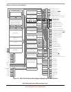
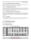
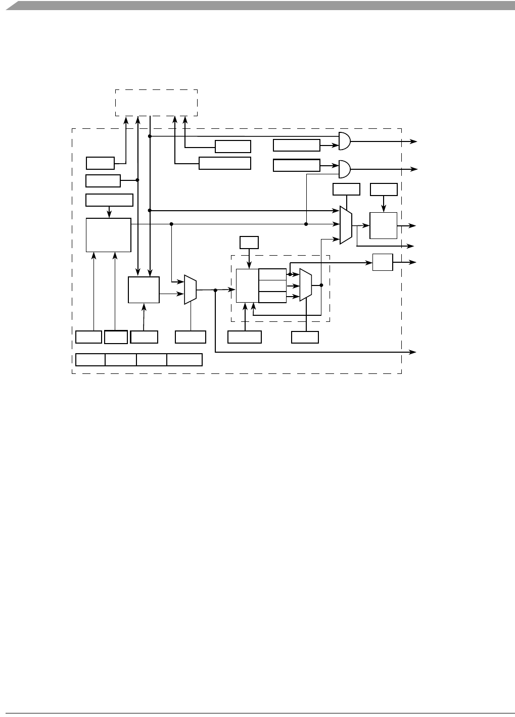
12.1.4 Block Diagram
Figure 12-2 is the ICS block diagram.
Figure 12-2. Internal Clock Source (ICS) Block Diagram
12.1.5 Modes of Operation
There are seven modes of operation for the ICS: FEI, FEE, FBI, FBILP, FBE, FBELP, and stop.
12.1.5.1 FLL Engaged Internal (FEI)
In FLL engaged internal mode, which is the default mode, the ICS supplies a clock derived from the FLL
controlled by the internal reference clock. The BDC clock is supplied from the FLL.
12.1.5.2 FLL Engaged External (FEE)
In FLL engaged external mode, the ICS supplies a clock derived from the FLL controlled by an external
reference clock. The BDC clock is supplied from the FLL.
12.1.5.3 FLL Bypassed Internal (FBI)
In FLL bypassed internal mode, the FLL is enabled and controlled by the internal reference clock, but is
bypassed. The ICS supplies a clock derived from the internal reference clock. The BDC clock is supplied
from the FLL.
RDIV
TRIM
/ 2
External Reference
IREFS
Clock
CLKS
n=0–10
/ 2
n
n=0–3
/ 2
n
Internal
Reference
Clock
BDIV
ICSLCLK
ICSOUT
ICSIRCLK
EREFS
RANGE
EREFSTENHGO
IREFSTEN
ICSERCLK
Internal Clock Source Block
ICSFFCLK
ERCLKEN
IRCLKEN
DCOOUT
DCOL
DCOM
DCOH
Filter
DRS
LP
FLL
DMX32FTRIM
DRST IREFST CLKST OSCINIT
ICSDCLK