


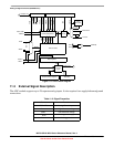
Analog-to-Digital Converter (S08ADC12V1)
MCF51QE128 MCU Series Reference Manual, Rev. 3
226 Freescale Semiconductor
Get the latest version from freescale.com
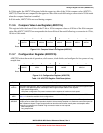
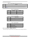
11.3.8 Pin Control 1 Register (APCTL1)
The pin control registers disable the I/O port control of MCU pins used as analog inputs. APCTL1 is
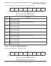
3:2
MODE
Conversion Mode Selection. MODE bits are used to select between 12-, 10-, or 8-bit operation. See Table 11-8.
1:0
ADICLK
Input Clock Select. ADICLK bits select the input clock source to generate the internal clock ADCK. See
Ta bl e 1 1- 9.
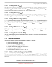
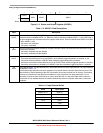
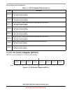
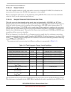
Table 11-7. Clock Divide Select
ADIV Divide Ratio Clock Rate
00 1 Input clock
01 2 Input clock ÷ 2
10 4 Input clock ÷ 4
11 8 Input clock ÷ 8
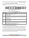
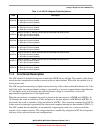
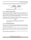
Table 11-8. Conversion Modes
MODE Mode Description
00 8-bit conversion (N=8)
01 12-bit conversion (N=12)
10 10-bit conversion (N=10)
11 Reserved
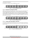
Table 11-9. Input Clock Select
ADICLK Selected Clock Source
00 Bus clock
01 Bus clock divided by 2
10 Alternate clock (ALTCLK)
11 Asynchronous clock (ADACK)
Table 11-6. ADCCFG Register Field Descriptions (continued)
Field Description