


Chapter 18 Version 1 ColdFire Debug (CF1_DEBUG)
MCF51QE128 MCU Series Reference Manual, Rev. 3
418 Freescale Semiconductor
Get the latest version from freescale.com
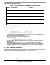
18.4.3.4.2 Supervisor Instruction Set
The supervisor instruction set has complete access to the user mode instructions plus the opcodes shown
below. The PST/DDATA specification for these opcodes is shown in Table 18-28.
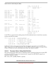
tpf PST = 0x01
tpf.l #<data> PST = 0x01
tpf.w #<data> PST = 0x01
trap #<data> PST = 0x01
1
tst.b <ea>x PST = 0x01, {PST = 0x08, DD = source operand}
tst.l <ea>y PST = 0x01, {PST = 0x0B, DD = source operand}
tst.w <ea>y PST = 0x01, {PST = 0x09, DD = source operand}
unlk Ax PST = 0x01, {PST = 0x0B, DD = destination operand}
wddata.b <ea>y PST = 0x04, PST = 0x08, DD = source operand
wddata.l <ea>y PST = 0x04, PST = 0x0B, DD = source operand
wddata.w <ea>y PST = 0x04, PST = 0x09, DD = source operand
1
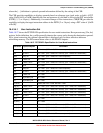
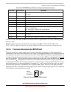
During normal exception processing, the PSTB is loaded with two successive 0x1C entries indicating the exception
processing state. The exception stack write operands, as well as the vector read and target address of the exception
handler may also be displayed.
Exception Processing:
PST = 0x1C, 0x1C,
{PST = 0x0B,DD = destination}, // stack frame
{PST = 0x0B,DD = destination}, // stack frame
{PST = 0x0B,DD = source}, // vector read
PST = 0x05,{PST = [0x0{DE}],DD = target}// handler PC
A similar set of PST/DD values is generated in response to an emulator mode excetion. For these events (caused
by a debug interrupt or properly-enabled trace exception), the initial PST values are 0x1D, 0x1D and the remaining
sequence is equivalent to normal exception processing.
The PST
/DDATA specification for the reset exception is shown below:
Exception Processing:
PST = 0x1C, 0x1C,
PST = 0x05,{PST = [0x0{DE}],DD = target}// handler PC
The initial references at address 0 and 4 are never captured nor displayed since these accesses are treated as
instruction fetches.
For all types of exception processing, the PST = 0x1C (or 0x1D) value is driven for two trace buffer entries.
2
For JMP and JSR instructions, the optional target instruction address is displayed only for those effective address
fields defining variant addressing modes. This includes the following <ea>x values: (An), (d16,An), (d8,An,Xi),
(d8,PC,Xi).
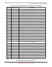
Table 18-27. PST/DDATA Specification for User-Mode Instructions (continued)
Instruction Operand Syntax PST/DDATA