


Chapter 18 Version 1 ColdFire Debug (CF1_DEBUG)
MCF51QE128 MCU Series Reference Manual, Rev. 3
Freescale Semiconductor 371
Get the latest version from freescale.com
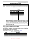
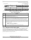
18.3.5 BDM Address Attribute Register (BAAR)
BAAR defines the address space for memory-referencing BDM commands. BAAR[R, SZ] are loaded
directly from the BDM command, while the lower five bits can be programmed from the external
development system. BAAR is loaded any time AATR is written and is initialized to a value of 0x05,
setting supervisor data as the default address space. The upper 24 bits of this register are reserved for future
use and any attempted write of these bits is ignored.
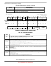
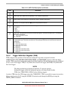
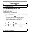
DRc: 0x03 (CSR3) Access: Supervisor write-only
BDM read/write
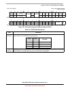
31 30 29 28 27 26 25 24 23 22 21 20 19 18 17 16
R 0
BFC
DIV8
BFCDIV
0000
0 000
W
Reset0000000000000000
1514131211109876543210
R 0 000000000 0 0 0000
W
Reset0000000000000000
Figure 18-6. Configuration/Status Register 3 (CSR3)
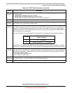
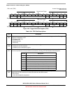
Table 18-11. CSR3 Field Descriptions
Field Description
31 Reserved, must be cleared.
30
BFCDIV8
BDM flash clock divide by 8.
0 Input to the flash clock divider is the bus clock
1 Input to the flash clock divider is the bus clock divided by 8
29–24
BFCDIV
BDM flash clock divider. The BFCDIV8 and BFCDIV fields specify the frequency of the internal flash clock when
performing a mass erase operation initiated by setting XCSR[ERASE]. These fields must be loaded with the
appropriate values prior to the setting of XCSR[ERASE] to initiate a mass erase operation in the flash memory.
This field divides the bus clock (or the bus clock divided by 8 if BFCDIV8 is set) by the value defined by the
BFCDIV plus one. The resulting frequency of the internal flash clock must fall within the range of 150–200 kHz for
proper flash operations. Program/erase timing pulses are one cycle of this internal flash clock, which corresponds
to a range of 5–6.7 µs. The automated programming logic uses an integer number of these pulses to complete
an erase or program operation.
if BFCDIV8 = 0, then f
FCLK
= f
Bus
÷ (BFCDIV + 1)
if BFCDIV8 = 1, then f
FCLK
= f
Bus
÷ (8 × (BFCDIV + 1)
where f
FCLK
is the frequency of the flash clock and f
Bus
is the frequency of the bus clock.
23–0 Reserved for future use by the debug module, must be cleared.