


MCF51QE128 MCU Series Reference Manual, Rev. 3
Freescale Semiconductor 71
Get the latest version from freescale.com
Chapter 4 Memory
Flash memory is ideal for single-supply applications allowing for field reprogramming without requiring
external high voltage sources for program or erase operations. The flash module includes a memory
controller that executes commands to modify flash memory contents.
Array read access time is one bus cycle for bytes, aligned words, and aligned longwords. Multiple accesses
are needed for misaligned words and longword operands. For flash memory, an erased bit reads 1 and a
programmed bit reads 0. It is not possible to read from a flash block while any command is executing on
that specific flash block.
CAUTION
A flash block address must be in the erased state before being programmed.
Cumulative programming of bits within a flash block address is not allowed
except for status field updates required in EEPROM emulation applications.
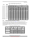
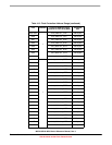
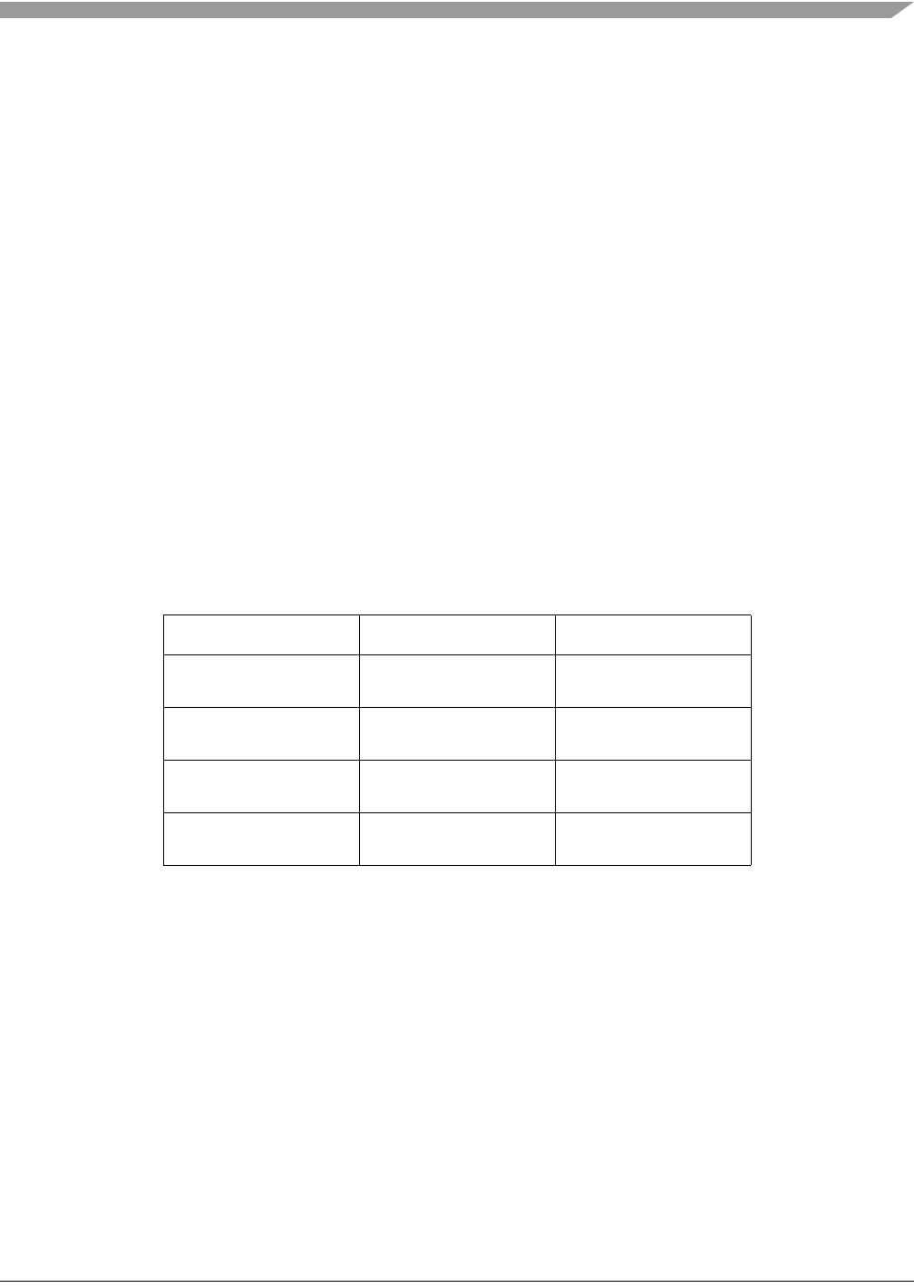
Flash memory on MCF51QE128/64/32 must be programmed 32-bits at a time when the low-voltage detect
flag (LVDF) in the system power management status and control 1 register (SPMSC1) is clear. If
SPMSC1[LVDF] is set, the programming sequence must be modified such that odd and even bytes are
written separately. The MCF51QE128/64/32 flash memory is organized as two 16-bit wide blocks
interleaved to yield a 32-bit data path. When programming flash when LVDF is set, alternate bytes must
be set to 0xFF as shown in Table 4-8. Failure to adhere to these guidelines may result in a partially
programmed flash array.
4.4.1 Features
Features of the flash memory include:
• Flash size
— MCF51QE128: 131,072 bytes (128 sectors of 1024 bytes each)
— MCF51QE64: 65,536 bytes (64 sectors of 1024 bytes each)
— MCF51QE32: 32,768 bytes (32 sectors of 1024 bytes each)
• Automated program and erase algorithm
• Fast program and sector erase operation
• Burst program command for faster flash array program times
• Single power supply program and erase
Table 4-8. Lov-Voltage Programming Sequence Example
Addresses Desired Value Values Programmed
0x00 – 0x03
0x00 – 0x03
0x5555_AAAA
0x55FF_AAFF
0xFF55_FFAA
0x04 – 0x07
0x04 – 0x07
0xCCCC_CCCC
0xCCFF_CCFF
0xFFCC_FFCC
0x08 – 0x0B
0x08 – 0x0B
0x1234_5678
0x12FF_56FF
0xFF34_FF78
0x0C – 0x0F
0x0C – 0x0F
0x9ABC_DEF0
0x9AFF_DEFF
0xFFBC_FFF0