Internal Clock Source (S08ICSV3)
MCF51QE128 MCU Series Reference Manual, Rev. 3
256 Freescale Semiconductor
Get the latest version from freescale.com
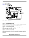
In FLL bypassed external mode, the ICSOUT clock is derived from the external reference clock. The
external reference clock controls the FLL clock, and the FLL loop locks the FLL frequency to the FLL
factor times the external reference frequency, as selected by the RDIV bits. The ICSLCLK is available for
BDC communications, and the external reference clock is enabled.
12.4.1.6 FLL Bypassed External Low Power (FBELP)
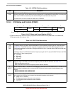
The FLL bypassed external low-power (FBELP) mode is entered when all the following conditions occur:
• CLKS bits are written to 10.
• IREFS bit is written to 0.
• BDM mode is not active and LP bit is written to 1.
In FLL bypassed external low power mode, the ICSOUT clock is derived from the external reference clock
and the FLL is disabled. The ICSLCLK is not available for BDC communications. The external reference
clock is enabled.
12.4.1.7 Stop
Stop mode is entered when the MCU enters a stop state. In this mode, all ICS clock signals are static except
in the following cases:
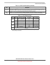
ICSIRCLK is active in stop mode when all the following conditions occur:
• IRCLKEN bit is written to 1
• IREFSTEN bit is written to 1
ICSERCLK is active in stop mode when all the following conditions occur:
• ERCLKEN bit is written to 1EREFSTEN bit is written to 1
12.4.2 Mode Switching
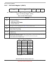
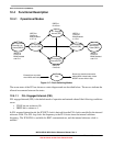
The IREF bit can be changed at anytime, but the actual switch to the newly selected clock is shown by the
IREFST bit. When switching between FLL engaged internal (FEI) and FLL engaged external (FEE)
modes, the FLL begins locking again after the switch is completed.
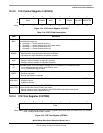
The CLKS bits can also be changed at anytime, but the actual switch to the newly selected clock is shown
by the CLKST bits. If the newly selected clock is not available, the previous clock remains selected.
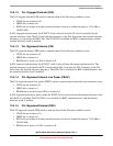
The DRS bits can be changed at anytime except when LP bit is 1. If the DRS bits are changed while in
FLL engaged internal (FEI) or FLL engaged external (FEE), the bus clock remains at the previous DCO
range until the new DCO starts. When the new DCO starts the bus clock switches to it. After switching to
the new DCO ,the FLL remains unlocked for several reference cycles. After the selected DCO startup time
is over, the FLL is locked. The completion of the switch is shown by the DRST bits.
12.4.3 Bus Frequency Divider
The BDIV bits can be changed at anytime and the actual switch to the new frequency occurs immediately.


