


Chapter 18 Version 1 ColdFire Debug (CF1_DEBUG)
MCF51QE128 MCU Series Reference Manual, Rev. 3
Freescale Semiconductor 389
Get the latest version from freescale.com
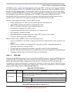
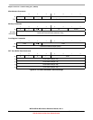
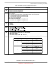
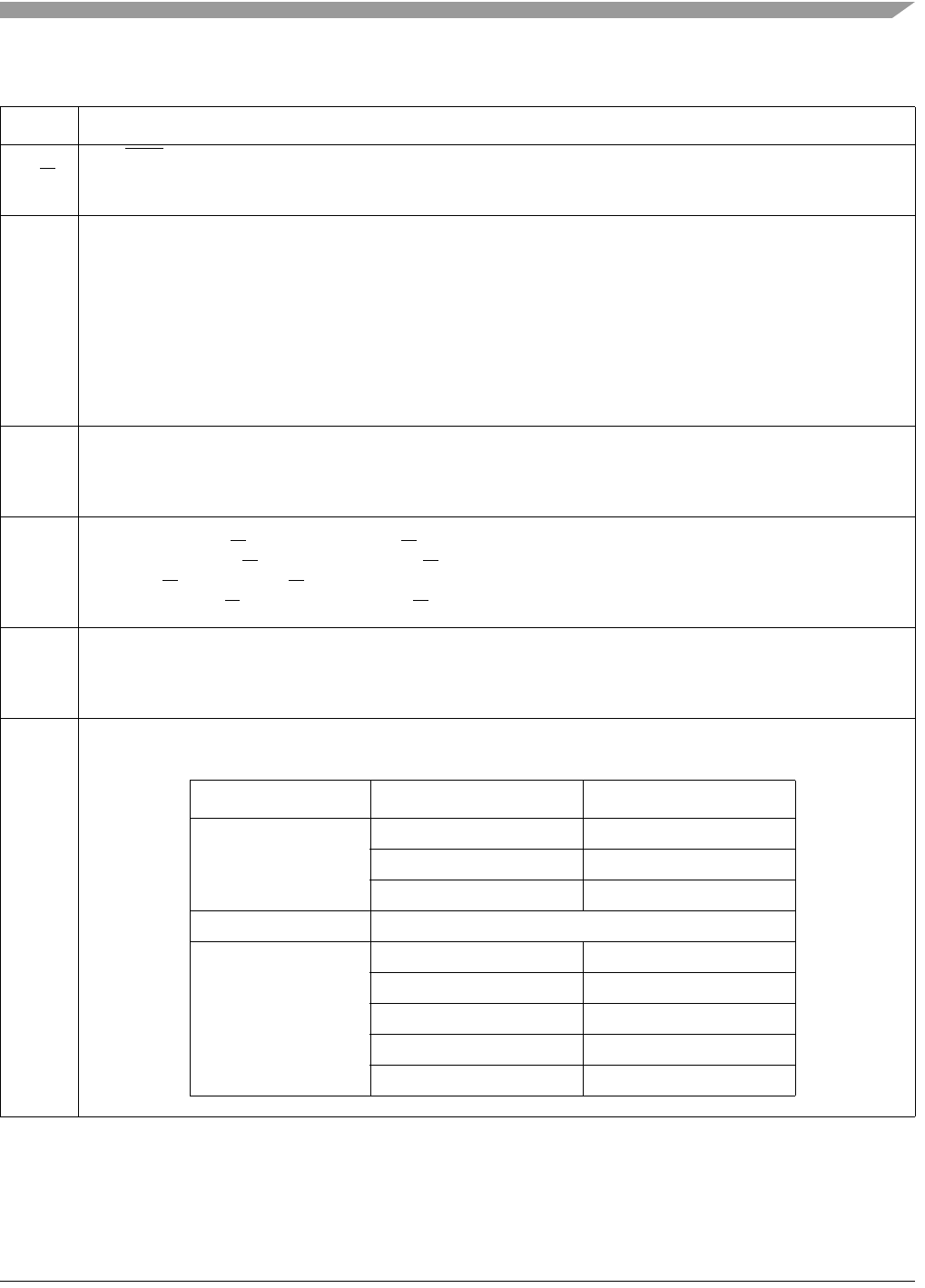
Table 18-24. BDM Command Code Field Descriptions
Field Description
5
R/W
Read/Write.
0 Command is performing a write operation.
1 Command is performing a read operation.
3–0
MSCMD
Miscellaneous command. Defines the miscellaneous command to be performed.
0000 No operation
0001 Display the CPU’s program counter (PC) plus optional capture in the PST trace buffer
0010 Enable the BDM acknowledge communication mode
0011 Disable the BDM acknowledge communication mode
0100 Force a CPU halt (background)
1000 Resume CPU execution (go)
1101 Read/write of the debug XCSR most significant byte
1110 Read/write of the debug CSR2 most significant byte
1111 Read/write of the debug CSR3 most significant byte
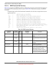
3–2
SZ
Memory operand size. Defines the size of the memory reference.
00 8-bit byte
01 16-bit word
10 32-bit long
1–0
MCMD
Memory command. Defines the type of the memory reference to be performed.
00 Simple write if R/W
= 0; simple read if R/W = 1
01 Write + status if R/W = 0; read + status if R/W = 1
10 Fill if R/W = 0; dump if R/W = 1
11 Fill + status if R/W
= 0; dump + status if R/W = 1
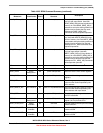
7–6
CRG
Core register group. Defines the core register group to be referenced.
01 CPU’s general-purpose registers (An, Dn) or PST trace buffer
10 DBG’s control registers
11 CPU’s control registers (PC, SR, VBR, CPUCR,...)
4–0
CRN
Core register number. Defines the specific core register (its number) to be referenced. All other CRN values are
reserved.
CRG CRN Register
01
0x00–0x07 D0–7
0x08–0x0F A0–7
0x10–0x1B PST Buffer 0–11
10 DRc[4:0] as described in Table 18-4
11
0x00 OTHER_A7
0x01 VBR
0x02 CPUCR
0x0E SR
0x0F PC