


MCF51QE128 MCU Series Reference Manual, Rev. 3
Freescale Semiconductor 29
Get the latest version from freescale.com
Chapter 1 Device Overview
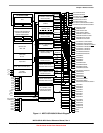
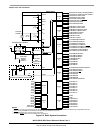
The ADC module also has an internally generated asynchronous clock that allows it to run in stop mode
(ADACK). This signal is not available externally and is not shown in this figure.
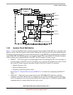
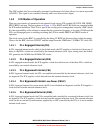
1.4.3 ICS Modes of Operation
There are seven modes of operation for the internal clock source (ICS) module: FEI, FEE, FBI, FBILP,
FBE, FBELP, and stop. These are shown in Figure 1-4. The IREFS and CLKS fields are contained within
the ICS module definition. The LP bit is part of the on-chip power management controller (PMC) block.
It is the responsibility of the software to ensure that the system bus frequency is less than 125 kHz and the
FLLs are disengaged prior to enabling switching the LP bit to enable FBELP and FBILP modes of
operation.
The clock source for the BDC is controlled by the debug CLKSW bit, discussed later in this document.
Choices for the BDC clock are ICSOUT and the output from the 10MHz bus / 20 MHz CPU clock FLL.
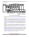
1.4.3.1 FLL Engaged Internal (FEI)
In FLL engaged internal mode, which is the default mode, the ICS supplies a clock derived from one of
three on chip FLLs, which are controlled by the internal reference clock. Upon exiting reset, the default
FLL generates the 10 MHz bus/20 MHz CPU clocks.
1.4.3.2 FLL Engaged External (FEE)
In FLL engaged external mode, the ICS supplies a clock derived from one of the three FLLs, which are
controlled by an external reference clock.
1.4.3.3 FLL Bypassed Internal (FBI)
In FLL bypassed internal mode, the FLLs are enabled and controlled by the internal reference clock, but
are bypassed. The ICS supplies a clock derived from the internal reference clock.
1.4.3.4 FLL Bypassed Internal Low-Power (FBILP)
In FLL bypassed internal low-power mode, the FLLs are disabled and bypassed, and the ICS supplies a
clock derived from the internal reference clock.
1.4.3.5 FLL Bypassed External (FBE)
In FLL bypassed external mode, the FLLs are enabled and controlled by an external reference clock, but
are bypassed. The ICS supplies a clock derived from the external reference clock. The external reference
clock can be an external crystal/resonator supplied by an OSC controlled by the ICS, or it can be another
external clock source.