


MCF51QE128 MCU Series Reference Manual, Rev. 3
Freescale Semiconductor 291
Get the latest version from freescale.com
Chapter 15
Serial Communications Interface (S08SCIV4)
15.1 Introduction
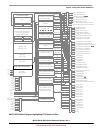
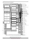
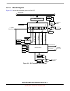
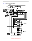
Figure 15-1 shows the MCF51QE128 Series block diagram with the SCI highlighted.
NOTE
Ignore any references to stop1 low-power mode in this chapter, because the
MCF51QE128 device does not support it.
15.1.1 SCI Clock Gating
The bus clock to SCI1 and SCI2 can be gated on and off using the SCGC1[SCI1,SCI2] bits, respectively.
These bits are set after any reset, which enables the bus clock to these modules. To conserve power, these
bits can be cleared to disable the clock to either of these modules when not in use. See Section 5.6,
“Peripheral Clock Gating,” for details.
15.1.2 Interrupt Vectors
Each SCI module contains three interrupt sources: transmit, receive, and error. See Chapter 8, “Interrupt
Controller (CF1_INTC),” for a list of the SCI interrupt vector assignments.