


MCF51QE128 MCU Series Reference Manual, Rev. 3
Freescale Semiconductor 129
Get the latest version from freescale.com
Chapter 6 Parallel Input/Output Control
6.7.5.2 Port E Data Direction Register (PTEDD)
6.7.5.3 Port E Data Set Register (PTESET)
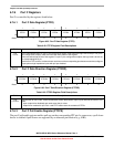
Table 6-24. PTED Register Field Descriptions
Field Description
7–0
PTEDn
Port E Data Register Bits. For port E pins configured as inputs, reads return the logic level on the pin. For port E
pins configured as outputs, reads return the last value written to this register.
Writes are latched into all bits of this register. For port E pins configured as outputs, the logic level is driven out
the corresponding MCU pin.
Reset forces PTED to all 0s, but these 0s are not driven out the corresponding pins because reset also configures
all port pins as high-impedance inputs with pull-ups disabled.
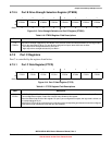
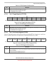
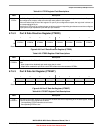
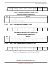
76543210
R
PTEDD7 PTEDD6 PTEDD5 PTEDD4 PTEDD3 PTEDD2 PTEDD1 PTEDD0
W
Reset:00000000
Figure 6-28. Port E Data Direction Register (PTEDD)
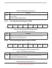
Table 6-25. PTEDD Register Field Descriptions
Field Description
7–0
PTEDDn
Data Direction for Port E Bits. These read/write bits control the direction of port E pins and what is read for PTED
reads.
0 Input (output driver disabled) and reads return the pin value.
1 Output driver enabled for port E bit n and PTED reads return the contents of PTEDn.
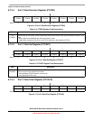
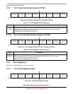
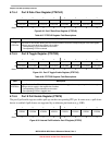
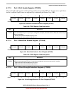
76543210
R
W PTESET7 PTESET6 PTESET5 PTESET4 PTESET3 PTESET2 PTESET1 PTESET0
Reset:00000000
Figure 6-29. Port E Data Set Register (PTESET)
Table 6-26. PTESET Register Field Descriptions
Field Description
7–0
PTESETn
Data Set for Port E Bits. Writing 1 to any bit in this location sets the corresponding bit in the data register. Writing
a zero to any bit in this register has no effect.
0 Corresponding PTEDn maintains current value.
1 Corresponding PTEDn is set.