


MCF51QE128 MCU Series Reference Manual, Rev. 3
Freescale Semiconductor 207
Get the latest version from freescale.com
Chapter 10
Analog Comparator 3V (ACMPVLPV1)
10.1 Introduction
MCF51QE128 Series MCUs have two independent analog comparators (ACMPs), named ACMP1 and
ACMP2.
The analog comparator module (ACMP) provides a circuit for comparing two analog input voltages or for
comparing one analog input voltage to an internal reference voltage. The comparator circuit is designed to
operate across the full range of the supply voltage (rail-to-rail operation).
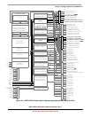
Figure 10-1 shows the MCF51QE128 Series block diagram with the ACMP highlighted.
NOTE
Ignore any references to stop1 low-power mode in this chapter, because the
MCF51QE128 device does not support it.
10.1.1 ACMP Configuration Information
When using the bandgap reference voltage for input to ACMP1+ and/or ACMP2+, enable the bandgap
buffer by setting SPMS[BGBE]. For value of bandgap voltage reference, see the data sheet.
10.1.2 ACMP/TPM Configuration Information
The ACMP modules can be configured to connect the output of the analog comparator to a TPM input
capture channel 0 by setting the corresponding ACICx bit in SOPT2. With ACICx set, the TPMxCH0 pin
is not available externally regardless of the configuration of the TPMx module.
The ACMP1 output can be connected to TPM1CH0. The ACMP2 output can be connected to TPM2CH0.
10.1.3 ACMP Clock Gating
The bus clock to both of the ACMPs can be gated on and off using the SCGC2[ACMP] bit. This bit is set
after any reset, which enables the bus clock to this module. To conserve power, the ACMP bit can be
cleared to disable the clock to this module when not in use. See Section 5.6, “Peripheral Clock Gating,”
for details.