


Analog-to-Digital Converter (S08ADC12V1)
MCF51QE128 MCU Series Reference Manual, Rev. 3
Freescale Semiconductor 235
Get the latest version from freescale.com
NOTE
Hexadecimal values designated by a preceding 0x, binary values designated
by a preceding %, and decimal values have no preceding character.
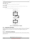
11.5.1 ADC Module Initialization Example
11.5.1.1 Initialization Sequence
Before the ADC module can be used to complete conversions, an initialization procedure must be
performed. A typical sequence is as follows:
1. Update the configuration register (ADCCFG) to select the input clock source and the divide ratio
used to generate the internal clock, ADCK. This register is also used for selecting sample time and
low-power configuration.
2. Update status and control register 2 (ADCSC2) to select the conversion trigger (hardware or
software) and compare function options, if enabled.
3. Update status and control register 1 (ADCSC1) to select whether conversions will be continuous
or completed only once, and to enable or disable conversion complete interrupts. The input channel
on which conversions will be performed is also selected here.
11.5.1.2 Pseudo-Code Example
In this example, the ADC module is set up with interrupts enabled to perform a single 10-bit conversion
at low power with a long sample time on input channel 1, where the internal ADCK clock is derived from
the bus clock divided by 1.
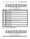
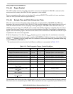
ADCCFG = 0x98 (%10011000)
Bit 7 ADLPC 1 Configures for low power (lowers maximum clock speed)
Bit 6:5 ADIV 00 Sets the ADCK to the input clock ÷ 1
Bit 4 ADLSMP 1 Configures for long sample time
Bit 3:2 MODE 10 Sets mode at 10-bit conversions
Bit 1:0 ADICLK 00 Selects bus clock as input clock source
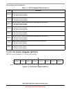
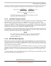
ADCSC2 = 0x00 (%00000000)
Bit 7 ADACT 0 Flag indicates if a conversion is in progress
Bit 6 ADTRG 0 Software trigger selected
Bit 5 ACFE 0 Compare function disabled
Bit 4 ACFGT 0 Not used in this example
Bit 3:2 00 Reserved, always reads zero
Bit 1:0 00 Reserved for Freescale’s internal use; always write zero
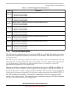
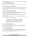
ADCSC1 = 0x41 (%01000001)
Bit 7 COCO 0 Read-only flag which is set when a conversion completes
Bit 6 AIEN 1 Conversion complete interrupt enabled
Bit 5 ADCO 0 One conversion only (continuous conversions disabled)
Bit 4:0 ADCH 00001 Input channel 1 selected as ADC input channel
ADCRH/L = 0xxx
Holds results of conversion. Read high byte (ADCRH) before low byte (ADCRL) so that
conversion data cannot be overwritten with data from the next conversion.