


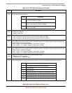

Chapter 18 Version 1 ColdFire Debug (CF1_DEBUG)
MCF51QE128 MCU Series Reference Manual, Rev. 3
Freescale Semiconductor 383
Get the latest version from freescale.com
The processor’s run/stop/halt status is always accessible in XCSR[CPUHALT,CPUSTOP]. Additionally,
CSR[27–24] indicate the halt source, showing the highest priority source for multiple halt conditions. This
field is cleared by a read of the CSR. The debug GO command also clears CSR[26–24].
18.4.1.2 Background Debug Serial Interface Controller (BDC)
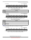
BDC serial communications use a custom serial protocol first introduced on the M68HC12 Family of
microcontrollers and later used in the M68HCS08 family. This protocol assumes that the host knows the
communication clock rate determined by the target BDC clock rate. The BDC clock rate may be the system
bus clock frequency or an alternate frequency source depending on the state of XCSR[CLKSW]. All
communication is initiated and controlled by the host which drives a high-to-low edge to signal the
beginning of each bit time. Commands and data are sent most significant bit (msb) first. For a detailed
description of the communications protocol, refer to Section 18.4.1.3, “BDM Communication Details”.
If a host is attempting to communicate with a target MCU that has an unknown BDC clock rate, a SYNC
command may be sent to the target MCU to request a timed synchronization response signal from which
the host can determine the correct communication speed. After establishing communications, the host can
read XCSR and write the clock switch (CLKSW) control bit to change the source of the BDC clock for
further serial communications if necessary.
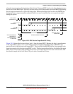
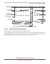
BKGD is a pseudo-open-drain pin and there is an on-chip pullup so no external pullup resistor is required.
Unlike typical open-drain pins, the external RC time constant on this pin, which is influenced by external
capacitance, plays almost no role in signal rise time. The custom protocol provides for brief, actively
driven speed-up pulses to force rapid rise times on this pin without risking harmful drive level conflicts.
Refer to Section 18.4.1.3, “BDM Communication Details,” for more details.
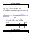
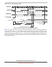
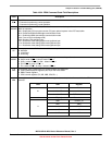
When no debugger pod is connected to the standard 6-pin BDM interface connector (Section 18.4.4,
“Freescale-Recommended BDM Pinout”), the internal pullup on BKGD chooses normal operating mode.
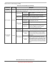
BKGD held low
for ≥2 bus clocks
after reset negated
for POR or BDM
reset
Immediate
Flash unsecure
Enters debug mode with XCSR[ENBDM, CLKSW] set. The full set of
BDM commands is available and debug can proceed.
If the core is reset into a debug halt condition, the processor’s response
to the GO command depends on the BDM command(s) performed while
it was halted. Specifically, if the PC register was loaded, the GO
command causes the processor to exit halted state and pass control to
the instruction address in the PC, bypassing normal reset exception
processing. If the PC was not loaded, the GO command causes the
processor to exit halted state and continue reset exception processing.
Flash secure
Enters debug mode with XCSR[ENBDM, CLKSW] set. The allowable
commands are limited to the always-available group. A GO command to
start the processor is not allowed. The only recovery actions in this mode
are:
• Issue a BDM reset setting CSR2[BDFR] with CSR2[BDHBR] cleared
and the BKGD pin held high
• Erase the flash to unsecure the memory and then proceed with debug
• Power cycle the device with the BKGD pin held high to reset into the
normal operating mode
Table 18-23. CPU Halt Sources (continued)
Halt Source Halt Timing Description