


MCF51QE128 MCU Series Reference Manual, Rev. 3
Freescale Semiconductor 203
Get the latest version from freescale.com
Chapter 9 Rapid GPIO (RGPIO)
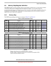
Figure 9-9. RGPIO Toggle Data Register (RGPIO_TOG)
9.4 Functional Description
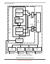
The RGPIO module is a relatively-simple design with its behavior controlled by the program-visible
registers defined within its programming model.
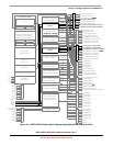
As shown in Figure 9-2, the RGPIO module is connected to the processor’s local two-stage pipelined bus
with the stages of the V1 ColdFire core’s operand execution pipeline (OEP) mapped directly onto the bus.
This structure allows the processor access to the RGPIO module for single-cycle pipelined reads and
writes with a zero wait-state response (as viewed in the system bus data phase stage).
9.5 Initialization Information
The reset state of the RGPIO module disables the entire 16-bit data port. Prior to using the RGPIO port,
software typically defines the contents of the data register (RGPIO_DATA), configure the pin direction
(RGPIO_DIR), and setting the appropriate bits in the pin enable register (RGPIO_ENB).
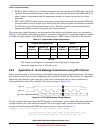
9.6 Application Information
In this section, the relative performance of the RGPIO output pins for two simple applications is examined.
In the first case, the processor executes a loop to toggle an output pin for a specific number of cycles. The
speed of the resulting square-wave output is studied. For the second example, the processor transmits a
16-bit message using a 3-pin SPI-like interface with a serial clock, serial chip select and serial data bit. In
both cases, the relative speed of the GPIO output is presented as a function of the location of the output bit
(RGPIO versus peripheral bus GPIO).
9.6.1 Application 1: Simple Square-Wave Generation
In this example, several different instruction loops are executed, each generating a square-wave output
with a 50% duty cycle. For this analysis, the executed code is mapped into the processor’s RAM. This
configuration is selected to remove any jitter from the output square wave caused by the limitations
defined by the two-cycle flash memory accesses and restrictions on the initiation of a flash access. The
following instruction loops were studied:
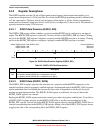
Offset: RGPIO_Base + 0xE (RGPIO_TOG) Access: Write-only
1514131211109876543210
R
WTOG
Reset————————————————
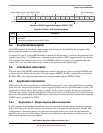
Table 9-10. RGPIO_TOG Field Descriptions
Field Description
15–0
TOG
RGPIO Toggle Data.
0 No effect.
1 Inverts the corresponding bit in RGPIO_DATA