


Analog-to-Digital Converter (S08ADC12V1)
MCF51QE128 MCU Series Reference Manual, Rev. 3
Freescale Semiconductor 237
Get the latest version from freescale.com
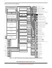
11.6.1.1 Analog Supply Pins
The ADC module has analog power and ground supplies (V
DDAD
and V
SSAD
) available as separate pins
on some devices. V
SSAD
is shared on the same pin as the MCU digital V
SS
on some devices.
On other
devices, V
SSAD
and V
DDAD
are shared with the MCU digital supply pins. In these cases, there are separate
pads for the analog supplies bonded to the same pin as the corresponding digital supply so that some degree
of isolation between the supplies is maintained.
When available on a separate pin, both V
DDAD
and V
SSAD
must be connected to the same voltage potential
as their corresponding MCU digital supply (V
DD
and V
SS
) and must be routed carefully for maximum
noise immunity and bypass capacitors placed as near as possible to the package.
If separate power supplies are used for analog and digital power, the ground connection between these
supplies must be at the V
SSAD
pin. This should be the only ground connection between these supplies if
possible. The V
SSAD
pin makes a good single point ground location.
11.6.1.2 Analog Reference Pins
In addition to the analog supplies, the ADC module has connections for two reference voltage inputs. The
high reference is V
REFH
, which may be shared on the same pin as V
DDAD
on some devices. The low
reference is V
REFL
, which may be shared on the same pin as V
SSAD
on some devices.
When available on a separate pin, V
REFH
may be connected to the same potential as V
DDAD
, or may be
driven by an external source between the minimum V
DDAD
spec and the V
DDAD
potential (V
REFH
must
never exceed V
DDAD
). When available on a separate pin, V
REFL
must be connected to the same voltage
potential as V
SSAD
. V
REFH
and V
REFL
must be routed carefully for maximum noise immunity and bypass
capacitors placed as near as possible to the package.
AC current in the form of current spikes required to supply charge to the capacitor array at each successive
approximation step is drawn through the V
REFH
and V
REFL
loop. The best external component to meet this
current demand is a 0.1 μF capacitor with good high frequency characteristics. This capacitor is connected
between V
REFH
and V
REFL
and must be placed as near as possible to the package pins. Resistance in the
path is not recommended because the current causes a voltage drop that could result in conversion errors.
Inductance in this path must be minimum (parasitic only).
11.6.1.3 Analog Input Pins
The external analog inputs are typically shared with digital I/O pins on MCU devices. The pin I/O control
is disabled by setting the appropriate control bit in one of the pin control registers. Conversions can be
performed on inputs without the associated pin control register bit set. It is recommended that the pin
control register bit always be set when using a pin as an analog input. This avoids problems with contention
because the output buffer is in its high impedance state and the pullup is disabled. Also, the input buffer
draws DC current when its input is not at V
DD
or V
SS
. Setting the pin control register bits for all pins used
as analog inputs should be done to achieve lowest operating current.
Empirical data shows that capacitors on the analog inputs improve performance in the presence of noise
or when the source impedance is high. Use of 0.01 μF capacitors with good high-frequency characteristics
is sufficient. These capacitors are not necessary in all cases, but when used they must be placed as near as
possible to the package pins and be referenced to V
SSA
.