


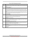


MCF51QE128 MCU Series Reference Manual, Rev. 3
306 Freescale Semiconductor
Get the latest version from freescale.com
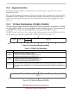
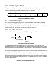
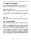
15.3.2 Transmitter Functional Description
This section describes the overall block diagram for the SCI transmitter, as well as specialized functions
for sending break and idle characters. The transmitter block diagram is shown in Figure 15-3.
The transmitter output (TxD) idle state defaults to logic high (TXINV is cleared following reset). The
transmitter output is inverted by setting TXINV. The transmitter is enabled by setting the TE bit in SCIxC2.
This queues a preamble character that is one full character frame of the idle state. The transmitter then
remains idle until data is available in the transmit data buffer. Programs store data into the transmit data
buffer by writing to the SCI data register (SCIxD).
The central element of the SCI transmitter is the transmit shift register that is 10 or 11 bits long depending
on the setting in the M control bit. For the remainder of this section, assume M is cleared, selecting the
normal 8-bit data mode. In 8-bit data mode, the shift register holds a start bit, eight data bits, and a stop
bit. When the transmit shift register is available for a new SCI character, the value waiting in the transmit
data register is transferred to the shift register (synchronized with the baud rate clock) and the transmit data
register empty (TDRE) status flag is set to indicate another character may be written to the transmit data
buffer at SCIxD.
If no new character is waiting in the transmit data buffer after a stop bit is shifted out the TxD pin, the
transmitter sets the transmit complete flag and enters an idle mode, with TxD high, waiting for more
characters to transmit.
Writing 0 to TE does not immediately release the pin to be a general-purpose I/O pin. Any transmit activity
in progress must first be completed. This includes data characters in progress, queued idle characters, and
queued break characters.
15.3.2.1 Send Break and Queued Idle
The SBK control bit in SCIxC2 sends break characters originally used to gain the attention of old teletype
receivers. Break characters are a full character time of logic 0 (10 bit times including the start and stop
bits). A longer break of 13 bit times can be enabled by setting BRK13. Normally, a program would wait
for TDRE to become set to indicate the last character of a message has moved to the transmit shifter, then
write 1 and then write 0 to the SBK bit. This action queues a break character to be sent as soon as the shifter
is available. If SBK remains 1 when the queued break moves into the shifter (synchronized to the baud rate
clock), an additional break character is queued. If the receiving device is another Freescale Semiconductor
SCI, the break characters are received as 0s in all eight data bits and a framing error (FE = 1) occurs.
When idle-line wakeup is used, a full character time of idle (logic 1) is needed between messages to wake
up any sleeping receivers. Normally, a program would wait for TDRE to become set to indicate the last
character of a message has moved to the transmit shifter, then write 0 and then write 1 to the TE bit. This
action queues an idle character to be sent as soon as the shifter is available. As long as the character in the
shifter does not finish while TE is cleared, the SCI transmitter never actually releases control of the TxD
pin. If there is a possibility of the shifter finishing while TE is cleard, set the general-purpose I/O controls
so the pin that is shared with TxD is an output driving a logic 1. This ensures that the TxD line looks like
a normal idle line even if the SCI loses control of the port pin between writing 0 and then 1 to TE.
The length of the break character is affected by the BRK13 and M bits as shown below.