


MCF51QE128 MCU Series Reference Manual, Rev. 3
102 Freescale Semiconductor
Get the latest version from freescale.com
Chapter 5 Resets, Interrupts, and General System Control
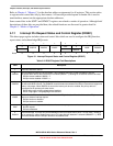
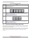
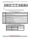
5.7.5 System Device Identification Register (SDIDH, SDIDL)
These high page read-only registers are included so host development systems can identify the ColdFire
derivative. This allows the development software to recognize where specific memory blocks, registers,
and control bits are located in a target MCU.
Additional configuration information about the ColdFire core and memory system is loaded into the 32-bit
D0 and D1 registers at reset. This information can be stored into memory by the system startup code for
later use by configuration-sensitive application code. See Chapter 7, “ColdFire Core,” for more
information.
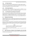
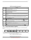
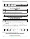
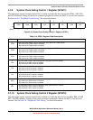
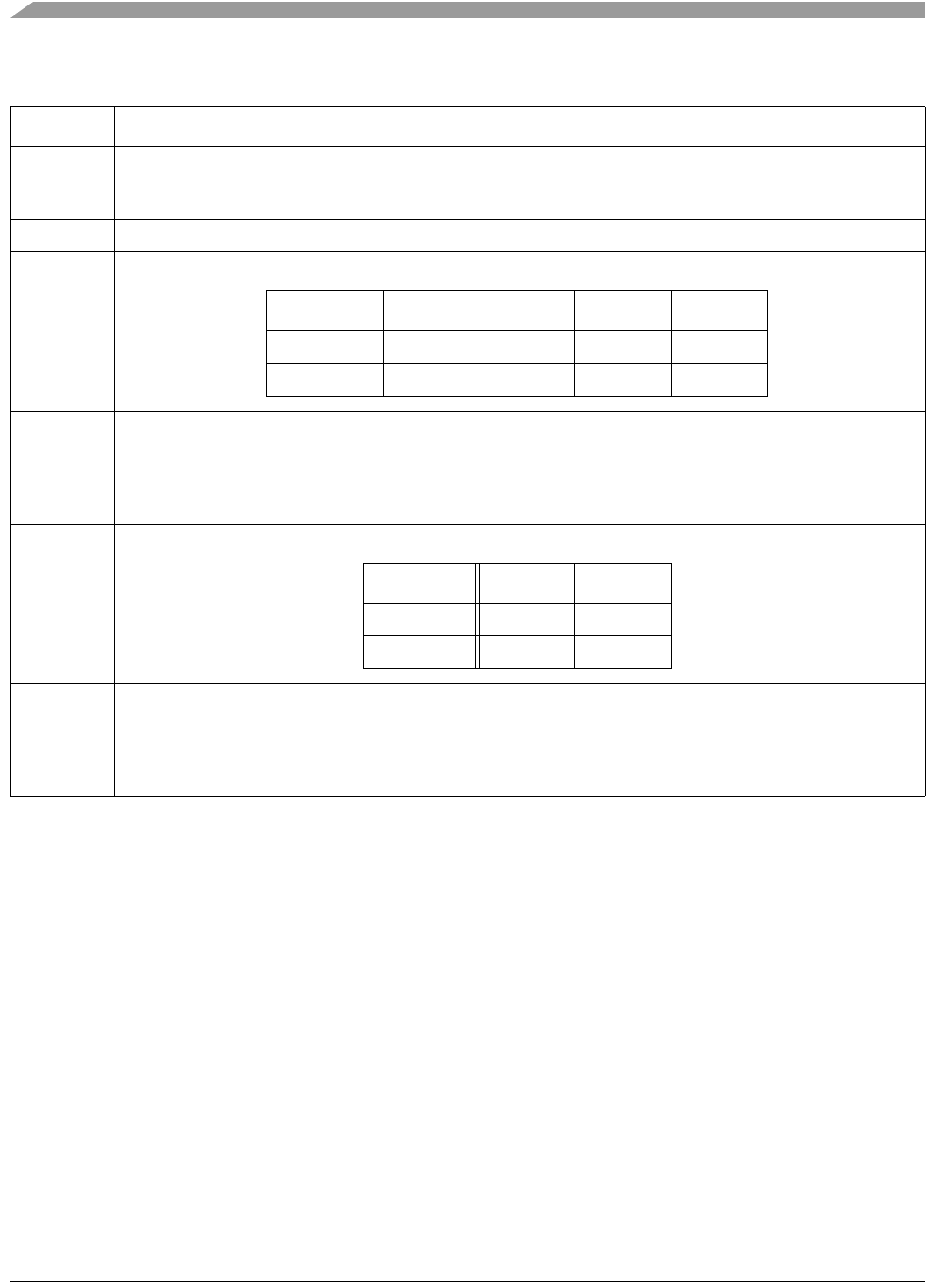
Table 5-5. SOPT2 Register Field Descriptions
Field Description
7
COPCLKS
COP Watchdog Clock Select. This write-once bit selects the clock source of the COP watchdog.
0 Internal 1-kHz clock is source to COP.
1 Bus clock is source to COP.
6–4 Reserved, should be cleared.
3
SPI1PS
SPI1 Pin Select. This bit selects the location of the SPSCLK1, MOSI1, MISO1, and SS1 pins of the SPI1 module.
2
ACIC2
Analog Comparator 2 to Input Capture Enable. This bit connects the output of ACMP2 to TPM2 input channel 0.
See Chapter 10, “Analog Comparator 3V (ACMPVLPV1),” and Chapter 17, “Timer/Pulse-Width Modulator
(S08TPMV3),” for more details on this feature.
0 ACMP2 output not connected to TPM2 input channel 0.
1 ACMP2 output connected to TPM2 input channel 0.
1
IIC1PS
IIC1 Pin Select. This bit selects the location of the SDA1 and SCL1 pins of the IIC1 module.
0
ACIC1
Analog Comparator 1 to Input Capture Enable. This bit connects the output of ACMP1 to TPM1 input channel 0.
See Chapter 10, “Analog Comparator 3V (ACMPVLPV1),” and Chapter 17, “Timer/Pulse-Width Modulator
(S08TPMV3),” for more details on this feature.
0 ACMP output not connected to TPM1 input channel 0.
1 ACMP output connected to TPM1 input channel 0.
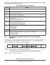
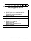
SPI1PS SPSCLK1 MOSI1 MISO1 SS1
0 PTB2 PTB3 PTB4 PTB5
1 PTE0 PTE1 PTE2 PTE3
IIC1PS SDA1 SCL1
0 PTA2 PTA3
1 PTB6 PTB7