


MCF51QE128 MCU Series Reference Manual, Rev. 3
Freescale Semiconductor 39
Get the latest version from freescale.com
Chapter 2 Pins and Connections
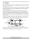
Although the BKGD/MS pin is a pseudo open-drain pin, the background debug communication protocol
provides brief, actively driven, high speed-up pulses to ensure fast rise times. Small capacitances from
cables and the absolute value of the internal pullup device play almost no role in determining rise and fall
times on the BKGD/MS pin.
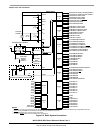
2.2.5 ADC Reference Pins (V
REFH
, V
REFL
)
The V
REFH
and V
REFL
pins are the voltage reference high and voltage reference low inputs, respectively,
for the ADC module.
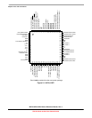
2.2.6 General-Purpose I/O and Peripheral Ports
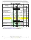
The MCF51QE128/64/32series of MCUs support up to 70 general-purpose I/O pins, 1 input-only pin, and
1 output-only pin, which are shared with on-chip peripheral functions (timers, serial I/O, ADC, ACMP,
etc.).
When a port pin is configured as a general-purpose output or a peripheral uses the port pin as an output,
software can select one of two drive strengths and enable or disable slew rate control. When a port pin is
configured as a general-purpose input or a peripheral uses the port pin as an input, software can enable a
pull-up device. Immediately after reset, all of these pins are configured as high-impedance
general-purpose inputs with internal pull-up devices enabled.
PTC4 is a special case I/O pin. When the PTC4/RGPIO12/TPM3CH4/RSTO pin is configured as RSTO,
it is an open drain output with an internal pullup. The voltage observed on the pin is not pulled to VDD,
and an external pullup resistor is recommended if this pin must drive off-chip signals.
PTA5/IRQ/TPM1CLK/RESET is also a special case I/O pin. It can only be configured as an input.
When an on-chip peripheral system is controlling a pin, data direction control bits still determine what is
read from the port data registers, even though the peripheral controls the pin direction via the pin’s output
buffer enable. For information about controlling these pins as general-purpose I/O pins, see Chapter 6,
“Parallel Input/Output Control”.
NOTE
To avoid extra current drain from floating input pins, the reset initialization
routine in the application program should enable on-chip pullup devices or
change the direction of unused or non-bonded pins to outputs so they do not
float.