


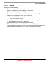
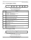
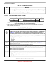
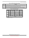


Internal Clock Source (S08ICSV3)
MCF51QE128 MCU Series Reference Manual, Rev. 3
Freescale Semiconductor 255
Get the latest version from freescale.com
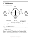
12.4.1.2 FLL Engaged External (FEE)
The FLL engaged external (FEE) mode is entered when all the following conditions occur:
• CLKS bits are written to 00.
• IREFS bit is written to 0.
• RDIV bits are written to divide external reference clock to be within the range of 31.25 kHz to
39.0625 kHz.
In FLL engaged external mode, the ICSOUT clock is derived from the FLL clock controlled by the
external reference clock.The FLL loop locks the frequency to the FLL factor times the external reference
frequency, as selected by the RDIV bits. The ICSLCLK is available for BDC communications, and the
external reference clock is enabled.
12.4.1.3 FLL Bypassed Internal (FBI)
The FLL bypassed internal (FBI) mode is entered when all the following conditions occur:
• CLKS bits are written to 01.
• IREFS bit is written to 1.
• BDM mode is active or LP bit is written to 0.
In FLL bypassed internal mode, the ICSOUT clock is derived from the internal reference clock. The
internal reference clock controls the FLL clock, and the FLL loop locks the FLL frequency to the FLL
factor times the internal reference frequency. The ICSLCLK is available for BDC communications, and
the internal reference clock is enabled.
12.4.1.4 FLL Bypassed Internal Low Power (FBILP)
The FLL bypassed internal low-power (FBILP) mode is entered when all the following conditions occur:
• CLKS bits are written to 01
• IREFS bit is written to 1.
• BDM mode is not active and LP bit is written to 1
In FLL bypassed internal low-power mode, the ICSOUT clock is derived from the internal reference clock
and the FLL is disabled. The ICSLCLK is not available for BDC communications, and the internal
reference clock is enabled.
12.4.1.5 FLL Bypassed External (FBE)
The FLL bypassed external (FBE) mode is entered when all the following conditions occur:
• CLKS bits are written to 10.
• IREFS bit is written to 0.
• RDIV bits are written to divide external reference clock to be within the range of 31.25 kHz to
39.0625 kHz.
• BDM mode is active or LP bit is written to 0.