


MCF51QE128 MCU Series Reference Manual, Rev. 3
Freescale Semiconductor 201
Get the latest version from freescale.com
Chapter 9 Rapid GPIO (RGPIO)
Figure 9-5. RGPIO Data Register (RGPIO_DATA)
9.3.2.3 RGPIO Pin Enable (RGPIO_ENB)
The RGPIO_ENB register indicates the corresponding package pin is to be configured as a RGPIO pin
instead of the normal GPIO pin mapped onto the peripheral bus.
The RGPIO_ENB register is read/write. At reset, all bits in the RGPIO_ENB are cleared, disabling the
RGPIO functionality.
Figure 9-6. RGPIO Enable Register (RGPIO_ENB)
9.3.2.4 RGPIO Clear Data (RGPIO_CLR)
The RGPIO_CLR register provides a mechanism to clear specific bits in the RGPIO_DATA by performing
a simple write. Clearing a bit in RGPIO_CLR clears the corresponding bit in the RGPIO_DATA register.
Setting it has no effect. The RGPIO_CLR register is write-only; reads of this address return the
RGPIO_DATA register.
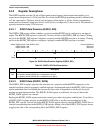
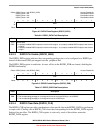
Offset: RGPIO_Base + 0x2 (RGPIO_DATA)
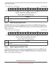
RGPIO_Base + 0x6
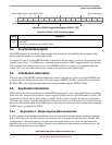
RGPIO_Base + 0xA
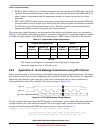
RGPIO_Base + 0xE
Access: Read/write
Read/Indirect Write
Read/Indirect Write
Read/Indirect Write
1514131211109876543210
R
DATA
W
Reset0000000000000000
Table 9-6. RGPIO_DATA Field Descriptions
Field Description
15–0
DATA
RGPIO data.
0 A properly-enabled RGPIO output pin is driven with a logic 0, or a properly-enabled RGPIO input pin was read as
a logic 0.
1 A properly-enabled RGPIO output pin is driven with a logic 1, or a properly-enabled RGPIO input pin was read as
a logic 1.
Offset: RGPIO_Base + 0x4 (RGPIO_ENB) Access: Read/write
1514131211109876543210
R
ENB
W
Reset0000000000000000
Table 9-7. RGPIO_ENB Field Descriptions
Field Description
15–0
ENB
RGPIO enable.
0 The corresponding package pin is configured for use as a normal GPIO pin, not a RGPIO.
1 The corresponding package pin is configured for use as a RGPIO pin.