


Timer/PWM Module (S08TPMV3)
MCF51QE128 MCU Series Reference Manual, Rev. 3
346 Freescale Semiconductor
Get the latest version from freescale.com
17.3.5 TPM Channel Value Registers (TPMxCnVH:TPMxCnVL)
These read/write registers contain the captured TPM counter value of the input capture function or the
output compare value for the output compare or PWM functions. The channel registers are cleared by
reset.
In input capture mode, reading either byte (TPMxCnVH or TPMxCnVL) latches the contents of both bytes
into a buffer where they remain latched until the other half is read. This latching mechanism also resets
(becomes unlatched) when the TPMxCnSC register is written (whether BDM mode is active or not). Any
write to the channel registers is ignored during the input capture mode.
When BDM is active, the coherency mechanism is frozen (unless reset by writing to TPMxCnSC register)
so the buffer latches remain in the state they were in when the BDM became active, even if one or both
halves of the channel register are read while BDM is active. This assures that if the user was in the middle
of reading a 16-bit register when BDM became active, it reads the appropriate value from the other half of
the 16-bit value after returning to normal execution. The value read from the TPMxCnVH and
TPMxCnVL registers in BDM mode is the value of these registers and not the value of their read buffer.
In output compare or PWM modes, writing to either byte (TPMxCnVH or TPMxCnVL) latches the value
into a buffer. After both bytes are written, they are transferred as a coherent 16-bit value into the
timer-channel registers according to the value of CLKSB:CLKSA bits and the selected mode, so:
• If CLKSB and CLKSA are cleared, the registers are updated when the second byte is written.
• If CLKSB and CLKSA are not cleared and in output compare mode, the registers are updated after
the second byte is written and on the next change of the TPM counter (end of the prescaler
counting).
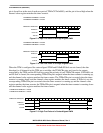
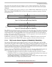
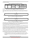
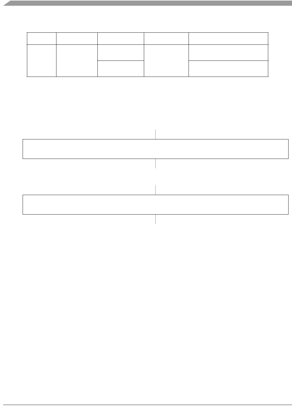
1XX
10
Center-aligned
PWM
High-true pulses
(clear output on compare-up)
X1
Low-true pulses
(set output on compare-up)
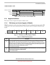
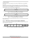
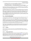
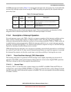
76543210
R
TPMxCnV[15:8]
W
Reset00000000
Figure 17-13. TPM Channel Value Register High (TPMxCnVH)
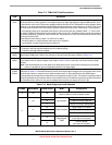
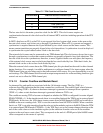
76543210
R
TPMxCnV[7:0]
W
Reset00000000
Figure 17-14. TPM Channel Value Register Low (TPMxCnVL)
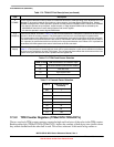
Table 17-6. Mode, Edge, and Level Selection (continued)
CPWMS MSnB:MSnA ELSnB:ELSnA Mode Configuration