


MCF51QE128 MCU Series Reference Manual, Rev. 3
Freescale Semiconductor 121
Get the latest version from freescale.com
6.7.2 Port B Registers
Port B is controlled by the registers listed below.
6.7.2.1 Port B Data Register (PTBD)
6.7.2.2 Port B Data Direction Register (PTBDD)
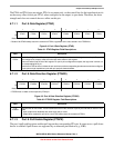
Table 6-5. PTADS Register Field Descriptions
Field Description
7–0
PTADSn
Output Drive Strength Selection for Port A Bits. Each of these control bits selects between low and high output
drive for the associated PTA pin. For port A pins configured as inputs, these bits have no effect.
0 Low output drive strength selected for port A bit n.
1 High output drive strength selected for port A bit n.
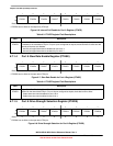
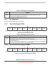
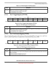
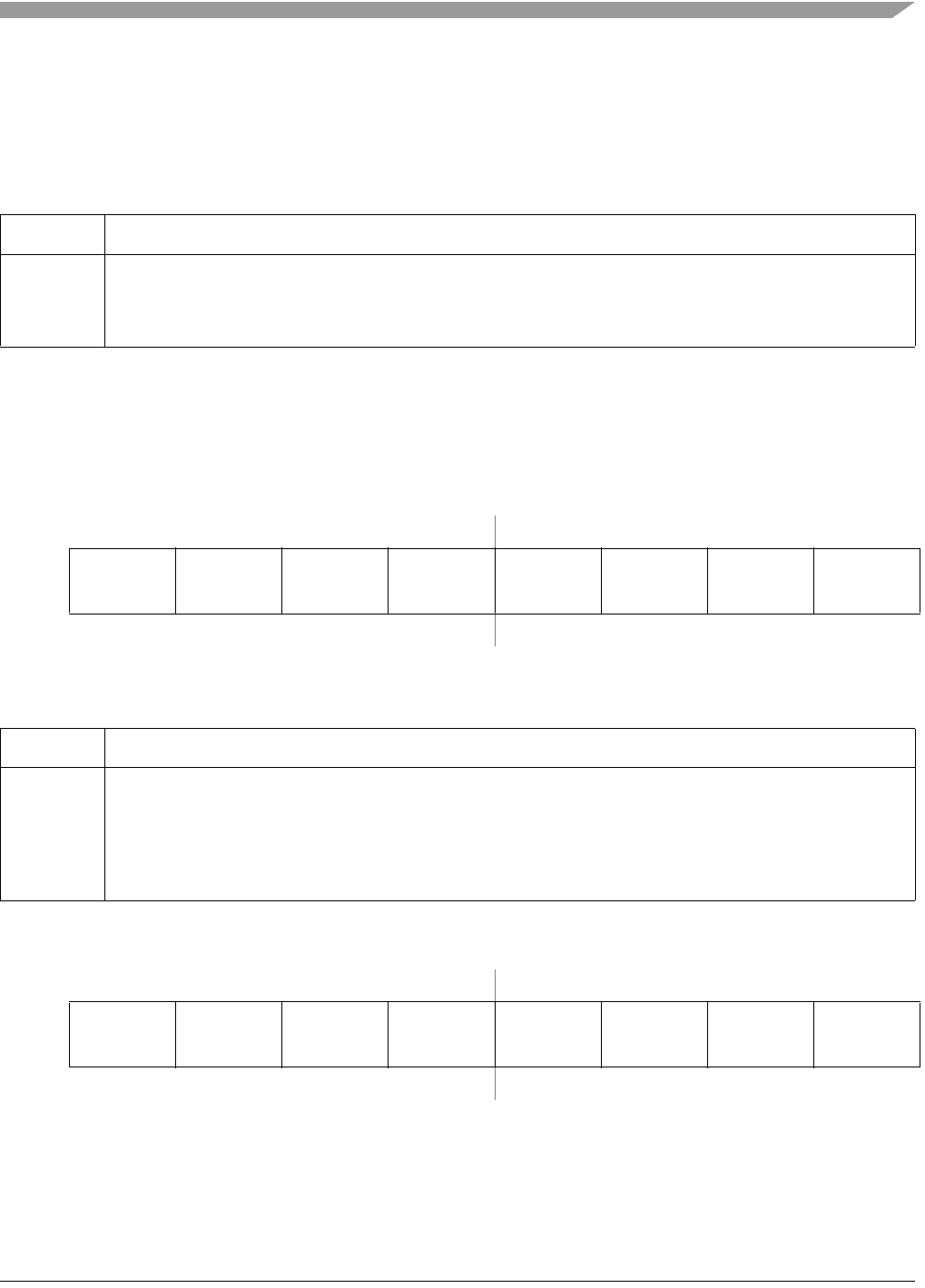
76543210
R
PTBD7 PTBD6 PTBD5 PTBD4 PTBD3 PTBD2 PTBD1 PTBD0
W
Reset:00000000
Figure 6-9. Port B Data Register (PTBD)
Table 6-6. PTBD Register Field Descriptions
Field Description
7–0
PTBDn
Port B Data Register Bits. For port B pins configured as inputs, reads return the logic level on the pin. For port B
pins configured as outputs, reads return the last value written to this register.
Writes are latched into all bits of this register. For port B pins configured as outputs, the logic level is driven out
the corresponding MCU pin.
Reset forces PTBD to all 0s, but these 0s are not driven out the corresponding pins because reset also configures
all port pins as high-impedance inputs with pull-ups/pull-downs disabled.
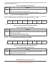
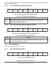
76543210
R
PTBDD7 PTBDD6 PTBDD5 PTBDD4 PTBDD3 PTBDD2 PTBDD1 PTBDD0
W
Reset:00000000
Figure 6-10. Port B Data Direction Register (PTBDD)