


Chapter 18 Version 1 ColdFire Debug (CF1_DEBUG)
MCF51QE128 MCU Series Reference Manual, Rev. 3
Freescale Semiconductor 359
Get the latest version from freescale.com
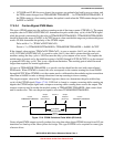
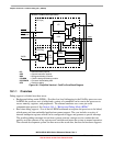
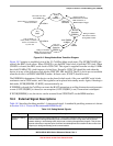
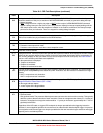
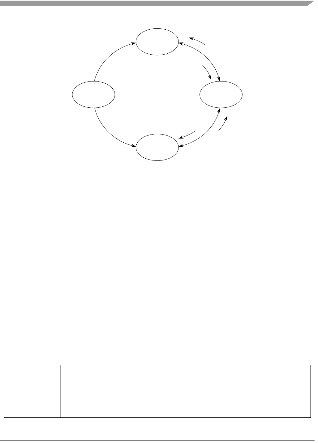
Figure 18-2. Debug Modes State Transition Diagram
Figure 18-2 contains a simplified view of the V1 ColdFire debug mode states. The XCSR[CLKSW] bit
controls the BDC clock source. When CLKSW is set, the BDC serial clock is half the CPU clock. When
CLKSW is cleared, the BDC serial clock is ICSLCLK. This signal is supplied from the on-chip 10 MHz
bus clock/20 MHz CPU clock frequency locked loop. Normally, ICSLCLK should be used when the
device in in any of the following clock modes: FBE, FEI, FBI, and FEE. The FLL clocks are not available
when the device is in FBELP and FBILP modes. In these cases, ICSOUT should be used.
The ENBDM bit determines if the device can be placed in halt mode, if the core and BDC serial clocks
continue to run in STOP modes, and if the regulator can be placed into standby mode. Again, if booting to
halt mode, XCSR[ENBDM, CLKSW] are automatically set.
If ENBDM is cleared, the ColdFire core treats the HALT instruction as an illegal instruction and generates
a reset (if CPUCR[IRD] is cleared) or an exception (if CPUCR[IRD] is set) if execution is attempted.
If XCSR[ENBDM] is set, the device can be restarted from STOP/WAIT via the BDM interface.
18.2 External Signal Descriptions
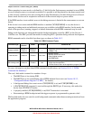
Table 18-3 describes the debug module’s 1-pin external signal. A standard 6-pin debug connector is shown
in Section 18.4.4, “Freescale-Recommended BDM Pinout”.
Table 18-3. Debug Module Signals
Signal Description
Background Debug
(BKGD)
Single-wire background debug interface pin. The primary function of this pin is for bidirectional serial
communication of background debug mode commands and data. During reset, this pin selects
between starting in active background (halt) mode or starting the application program. This pin also
requests a timed sync response pulse to allow a host development tool to determine the correct clock
frequency for background debug serial communications.
Debug
Halt
ENBDM=1
Normal
Operation
ENBDM=0
Normal
Operation
ENBDM=1
Any
State
CPU clock/2 is used
as the BDM clock
CLKSW=1
Return to Halt via
BACKGROUND command,
HALT instruction, or
BDM breakpoint trigger
BDM GO
command
clear ENBDM
via BDM
Set
ENBDM
Debug not enabled
BDM & CPU clocks are not
enabled in STOP modes
Debug is enabled
CPU clocks continue
during STOP modes
CLKSW=0
POR with BKGD=1 or
BDFR, BFHBR, and BKGD=1 or
BDFR=1 and BFHBR=0 or
any other reset
(POR or BDFR=1) with BKGD=0 or
BDFR and BFHBR= 1