


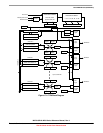

Timer/PWM Module (S08TPMV3)
MCF51QE128 MCU Series Reference Manual, Rev. 3
Freescale Semiconductor 339
Get the latest version from freescale.com
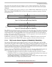
17.2.1.1 EXTCLK — External Clock Source
Control bits in the timer status and control register allow you to select nothing (timer disable), the bus-rate
clock (the normal default source), a crystal-related clock, or an external clock as the clock that drives the
TPM prescaler and subsequently the 16-bit TPM counter. The external clock source is synchronized in the
TPM. The bus clock clocks the synchronizer. The frequency of the external source must be no more than
one-fourth the frequency of the bus-rate clock to meet Nyquist criteria and allowing for jitter.
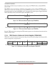
The external clock signal shares the same pin as a channel I/O pin, so the channel pin is not usable for
channel I/O function when selected as the external clock source. It is the your responsibility to avoid such
settings. If this pin is used as an external clock source (CLKSB:CLKSA = 1:1), the channel can remain in
output compare mode as a software timer (ELSnB:ELSnA = 0:0).
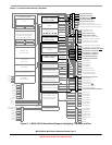
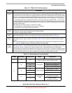
17.2.1.2 TPMxCHn — TPM Channel n I/O Pin(s)
Each TPM channel is associated with an I/O pin on the MCU. The function of this pin depends on the
channel configuration. The TPM pins share with general purpose I/O pins, where each pin has a port data
register bit, and a data direction control bit, and the port has optional passive pullups which may be enabled
when a port pin is acting as an input.
The TPM channel does not control the I/O pin when ELSnB:ELSnA or CLKSB:CLKSA are cleared so it
normally reverts to general purpose I/O control. When CPWMS is set and ELSnB:ELSnA are not cleared,
all channels within the TPM are configured for center-aligned PWM and the TPMxCHn pins are all
controlled by the TPM system. When CPWMS is cleared, the MSnB:MSnA control bits determine
whether the channel is configured for input capture, output compare, or edge-aligned PWM.
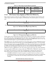
When a channel is configured for input capture (CPWMS=0, MSnB:MSnA = 0:0 and ELSnB:ELSnA not
= 0:0), the TPMxCHn pin is forced to act as an edge-sensitive input to the TPM. ELSnB:ELSnA control
bits determine what polarity edge or edges trigger input-capture events. A synchronizer based on the bus
clock synchronizes input edges to the bus clock. This implies the minimum pulse width—that can be
reliably detected—on an input capture pin is four bus clock periods (with ideal clock pulses as near as two
bus clocks can be detected). TPM uses this pin as an input capture input to override the port data and data
direction controls for the same pin.
When a channel is configured for output compare (CPWMS = 0, MSnB:MSnA = 01 and
ELSnB:ELSnA ≠ 00), the associated data direction control is overridden, the TPMxCHn pin is considered
an output controlled by the TPM, and the ELSnB:ELSnA control bits determine how the pin is controlled.
The remaining three combinations of ELSnB:ELSnA determine whether the TPMxCHn pin is toggled,
cleared, or set each time the 16-bit channel value register matches the timer counter.
When the output compare toggle mode is initially selected, the previous value on the pin is driven out until
the next output compare event, then the pin is toggled.
When a channel is configured for edge-aligned PWM (CPWMS = 0, MSnB = 1, ELSnB:ELSnA ≠ 00), the
data direction is overridden, the TPMxCHn pin is forced to be an output controlled by the TPM, and
ELSnA controls the polarity of the PWM output signal on the pin. When ELSnB is set and ELSnA is
cleared, the TPMxCHn pin is forced high at the start of each new period (TPMxCNT=0x0000). The pin is
forced low when the channel value register matches the timer counter. When ELSnA is set, the TPMxCHn