


MCF51QE128 MCU Series Reference Manual, Rev. 3
Freescale Semiconductor 113
Get the latest version from freescale.com
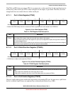
Chapter 6
Parallel Input/Output Control
This section explains software controls related to parallel input/output (I/O) and pin control. The
MCF51QE128/64 devices have up to nine parallel I/O ports that include a total of 70 I/O pins and one
input-only and one output-only pin. See Chapter 2, “Pins and Connections,” for more information about
pin assignments and external hardware considerations of these pins.
In addition to standard I/O port functionality, ports C and E have set/clear/toggle functions integrated as
part of the ColdFire core itself to improve edge resolution on those pins. See Section 6.4, “V1 ColdFire
Rapid GPIO Functionality,” and Chapter 9, “Rapid GPIO (RGPIO),” for additional details.
Many port pins are shared with on-chip peripherals such as timer systems, communication systems, or
keyboard interrupts as shown in Figure 1-1. The peripheral modules have priority over the general-purpose
I/O functions so that when a peripheral is enabled, the I/O functions associated with the shared pins may
be disabled.
After reset, the shared peripheral functions are disabled and the pins are configured as inputs
(PTxDDn = 0). The pin control functions for each pin are configured as follows: slew rate control disabled
(PTxSEn = 0), low drive strength selected (PTxDSn = 0), and internal pull-ups disabled (PTxPEn = 0).
NOTE
Not all general-purpose I/O pins are available on all packages. To avoid
extra current drain from floating input pins, the reset initialization routine in
the application program must enable on-chip pull-up devices or change the
direction of unconnected pins to outputs so the pins do not float.
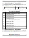
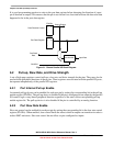
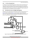
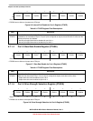
6.1 Port Data and Data Direction
Reading and writing of parallel I/Os are performed through the port data registers. The direction, input or
output, is controlled through the port data direction registers. The parallel I/O port function for an
individual pin is illustrated in the block diagram shown in Figure 6-1.
The data direction control bit (PTxDDn) determines whether the output buffer for the associated pin is
enabled and also controls the source for port data register reads. The input buffer for the associated pin is
always enabled unless the pin is enabled as an analog function or is an output-only pin.
When a shared digital function is enabled for a pin, the output buffer is controlled by the shared function.
However, the data direction register bit continues to control the source for reads of the port data register.
When a shared analog function is enabled for a pin, the input and output buffers are disabled. A value of
0 is read for any port data bit where the bit is an input (PTxDDn = 0) and the input buffer is disabled. In
general, when a pin is shared with an alternate digital function and an analog function, the analog function
has priority. Therefore, if the digital and analog functions are enabled, the analog function controls the pin.