


MCF51QE128 MCU Series Reference Manual, Rev. 3
90 Freescale Semiconductor
Get the latest version from freescale.com
Chapter 4 Memory
5. If any of the keys are written on successive MCU clock cycles.
6. Executing a STOP instruction before all keys have been written.
After the backdoor keys have been correctly matched, the MCU is unsecured. After the MCU is unsecured,
the flash security byte can be programmed to the unsecure state, if desired.
In the unsecure state, you have full control of the contents of the backdoor keys by programming the
associated addresses in the flash configuration field (see Section 4.2.1, “Flash Module Reserved Memory
Locations”).
The security as defined in the flash security byte is not changed by using the backdoor key access sequence
to unsecure. The stored backdoor keys are unaffected by the backdoor key access sequence. After the next
reset of the MCU, the security state of the flash module is determined by the flash security byte. The
backdoor key access sequence has no effect on the program and erase protections defined in the flash
protection register (FPROT).
It is not possible to unsecure the MCU by using the backdoor key access sequence in background debug
mode (BDM).
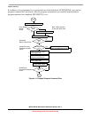
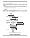
4.5.6 Resets
4.5.6.1 Flash Reset Sequence
On each reset, the flash module executes a reset sequence to hold CPU activity while reading the following
resources from the flash block:
• MCU control parameters (see Section 4.2.1)
• Flash protection byte (see Section 4.2.1 and Section 4.4.2.4)
• Flash nonvolatile byte (see Section 4.2.1)
• Flash security byte (see Section 4.2.1 and Section 4.4.2.2)
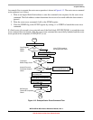
4.5.6.2 Reset While Flash Command Active
If a reset occurs while any flash command is in progress, that command is immediately aborted. The state
of the flash array address being programmed or the sector/block being erased is not guaranteed.
4.5.6.3 Program and Erase Times
Before any program or erase command can be accepted, the flash clock divider (FCDIV) must be written
to set the internal clock for the flash module to a frequency (f
FCLK
) between 150 kHz and 200 kHz.
If the initial flash event is a mass erase and verify from BDM, then CSR3[31:24] must be loaded before
the XCSR is written to initiate the erase and verify. The data in the XCSR and CSR3 is then loaded into
the flash’s FCDIV register. (See Section 18.3.4, “Configuration/Status Register 3 (CSR3)”). However, if
the first flash event is executed by the processor directly, the flash’s FCDIV register is written directly, and
the XCSR and CSR3 are not involved.