


MCF51QE128 MCU Series Reference Manual, Rev. 3
Freescale Semiconductor 69
Get the latest version from freescale.com
Chapter 4 Memory
to disengage security is by mass-erasing the flash (normally through the background debug interface) and
verifying the flash is blank.
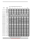
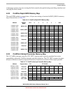
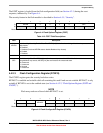
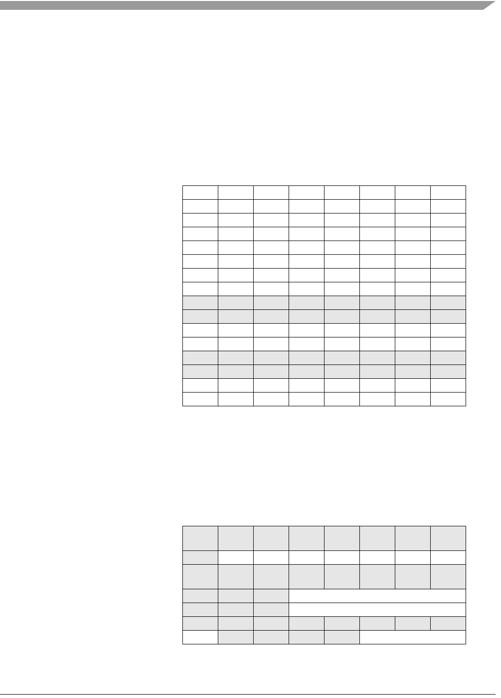
4.2.2 ColdFire Rapid GPIO Memory Map
The rapid GPIO module is mapped into a 16-byte area starting at location 0x(00)C0_0000. Its memory
map is shown below in Table 4-6.
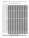
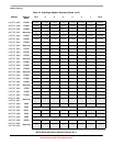
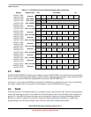
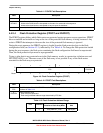
4.2.3 ColdFire Interrupt Controller Memory Map
The V1 ColdFire interrupt controller (CF1_INTC) register map is sparsely-populated, but retains
compatibility with earlier ColdFire interrupt controller definitions. The CF1_INTC occupies the upper
64 bytes of the device memory map and all memory locations are accessed as 8-bit (byte) operands.
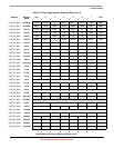
Table 4-6. V1 ColdFire Rapid GPIO Memory Map
Address
Register
Name
Bit 7654321Bit 0
0x(00)C0_0000
RGPIO_DIR
15 14 13 12 11 10 9 8
0x(00)C0_0001 76543210
0x(00)C0_0002
RGPIO_DATA
15 14 13 12 11 10 9 8
0x(00)C0_0003 76543210
0x(00)C0_0004
RGPIO_ENB
15 14 13 12 11 10 9 8
0x(00)C0_0005 76543210
0x(00)C0_0006
RGPIO_CLR
15 14 13 12 11 10 9 8
0x(00)C0_0007 76543210
0x(00)C0_0008
Reserved
— — — — — — — —
0x(00)C0_0009 — — — — — — — —
0x(00)C0_000A
RGPIO_SET
15 14 13 12 11 10 9 8
0x(00)C0_000B 76543210
0x(00)C0_000C
Reserved
— — — — — — — —
0x(00)C0_000D
— — — — — — — —
0x(00)C0_000E
RGPIO_TOG
15 14 13 12 11 10 9 8
0x(00)C0_000F 76543210
Table 4-7. V1 ColdFire Interrupt Controller Memory Map
Address Register Name msb Bit Number lsb
0x(FF)FF_FFC0–
0x(FF)FF_FFD2
Reserved
— — — — — — — —
0x(FF)FF_FFD3 INTC_FRC
0 LVL1 LVL2 LVL3 LVL4 LVL5 LVL6 LVL7
0x(FF)FF_FFD4–
0x(FF)FF_FFD7
Reserved
— — — — — — — —
0x(FF)FF_FFD8 INTC_PL6P7
0 0 0REQN
0x(FF)FF_FFD9 INTC_PL6P6
0 0 0REQN
0x(FF)FF_FFDA Reserved
— — — — — — — —
0x(FF)FF_FFDB INTC_WCR ENB
0 0 0 0MASK