


Timer/PWM Module (S08TPMV3)
MCF51QE128 MCU Series Reference Manual, Rev. 3
Freescale Semiconductor 347
Get the latest version from freescale.com
• If CLKSB and CLKSA are not cleared and in EPWM or CPWM modes, the registers are updated
after the both bytes were written, and the TPM counter changes from
TPMxMODH:TPMxMODL − 1 to TPMxMODH:TPMxMODL. If the TPM counter is a
free-running counter, the update is made when the TPM counter changes from 0xFFFE to 0xFFFF.
The latching mechanism may be manually reset by writing to the TPMxCnSC register (whether BDM
mode is active or not). This latching mechanism allows coherent 16-bit writes in big-endian or little-endian
order that is friendly to various compiler implementations.
When BDM is active, the coherency mechanism is frozen so the buffer latches remain in the state they
were in when the BDM became active even if one or both halves of the channel register are written while
BDM is active. Any write to the channel registers bypasses the buffer latches and directly write to the
channel register while BDM is active. The values written to the channel register while BDM is active are
used for PWM and output compare operation after normal execution resumes. Writes to the channel
registers while BDM is active do not interfere with partial completion of a coherency sequence. After the
coherency mechanism has been fully exercised, the channel registers are updated using the buffered values
written (while BDM was not active) by the user.
17.4 Functional Description
All TPM functions are associated with a central 16-bit counter that allows flexible selection of the clock
source and prescale factor. There is also a 16-bit modulo register associated with the main counter.
The CPWMS control bit chooses between center-aligned PWM operation for all channels in the TPM
(CPWMS=1) or general purpose timing functions (CPWMS=0) where each channel can independently be
configured to operate in input capture, output compare, or edge-aligned PWM mode. The CPWMS control
bit is located in the main TPM status and control register because it affects all channels within the TPM
and influences the way the main counter operates. (In CPWM mode, the counter changes to an up/down
mode rather than the up-counting mode used for general purpose timer functions.)
The following sections describe the main counter and each of the timer operating modes (input capture,
output compare, edge-aligned PWM, and center-aligned PWM). Because details of pin operation and
interrupt activity depend upon the operating mode, these topics are covered in the associated mode
explanation sections.
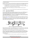
17.4.1 Counter
All timer functions are based on the main 16-bit counter (TPMxCNTH:TPMxCNTL). This section
discusses selection of the clock source, end-of-count overflow, up-counting vs. up/down counting, and
manual counter reset.
17.4.1.1 Counter Clock Source
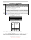
The 2-bit field, CLKSB:CLKSA, in the timer status and control register (TPMxSC) selects one of three
possible clock sources or OFF (which effectively disables the TPM). See Table 17-3. After any MCU reset,
CLKSB and CLKSA are cleared so no clock source is selected, and the TPM is in a very low power state.
These control bits may be read or written at any time and disabling the timer (writing 00 to the
CLKSB:CLKSA field) does not affect the values in the counter or other timer registers.