


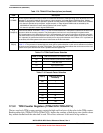
Timer/PWM Module (S08TPMV3)
MCF51QE128 MCU Series Reference Manual, Rev. 3
350 Freescale Semiconductor
Get the latest version from freescale.com
In output compare mode, values are transferred to the corresponding timer channel registers only after both
8-bit halves of a 16-bit register have been written and according to the value of CLKSB:CLKSA bits, so:
• If CLKSB:CLKSA are cleared, the registers are updated when the second byte is written
• If CLKSB:CLKSA are not cleared, the registers are updated at the next change of the TPM counter
(end of the prescaler counting) after the second byte is written.
The coherency sequence can be manually reset by writing to the channel status/control register
(TPMxCnSC).
An output compare event sets a flag bit (CHnF) which may optionally generate a CPU-interrupt request.
17.4.2.3 Edge-Aligned PWM Mode
This type of PWM output uses the normal up-counting mode of the timer counter (CPWMS=0) and can
be used when other channels in the same TPM are configured for input capture or output compare
functions. The period of this PWM signal is determined by the value of the modulus register
(TPMxMODH:TPMxMODL) plus 1. The duty cycle is determined by the setting in the timer channel
register (TPMxCnVH:TPMxCnVL). The polarity of this PWM signal is determined by the setting in the
ELSnA control bit. 0% and 100% duty cycle cases are possible.
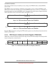
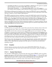
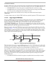
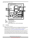
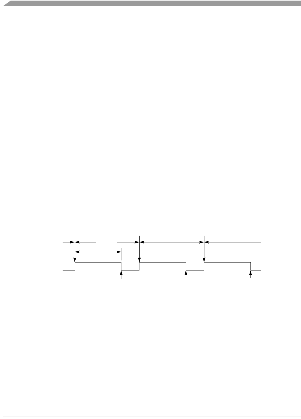
The output compare value in the TPM channel registers determines the pulse width (duty cycle) of the
PWM signal (Figure 17-15). The time between the modulus overflow and the output compare is the pulse
width. If ELSnA is cleared, the counter overflow forces the PWM signal high, and the output compare
forces the PWM signal low. If ELSnA is set, the counter overflow forces the PWM signal low, and the
output compare forces the PWM signal high.
Figure 17-15. PWM Period and Pulse Width (ELSnA=0)
When the channel value register is set to 0x0000, the duty cycle is 0%. A 100% duty cycle is achieved by
setting the timer-channel register (TPMxCnVH:TPMxCnVL) to a value greater than the modulus setting.
This implies that the modulus setting must be less than 0xFFFF to get 100% duty cycle.
Since the TPM is connected to an 8-bit peripheral bus, the settings in the timer channel registers are
buffered to ensure coherent 16-bit updates and to avoid unexpected PWM pulse widths. Writes to any of
the registers, TPMxCnVH and TPMxCnVL, actually writes to buffer registers. In edge-aligned PWM
mode, values are transferred to the corresponding timer-channel registers according to the value of
CLKSB:CLKSA bits:
• If CLKSB and CLKSA are cleared, the registers are updated when the second byte is written
Period
Pulse
Width
Overflow Overflow Overflow
Output
Compare
Output
Compare
Output
Compare
TPMxCHn