


ColdFire Core
MCF51QE128 MCU Series Reference Manual, Rev. 3
148 Freescale Semiconductor
NOTE
Registers D0 and D1 contain hardware configuration details after reset. See
Section 7.3.3.14, “Reset Exception” for more details.
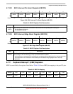
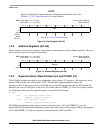
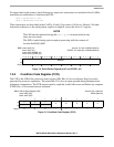
7.2.2 Address Registers (A0–A6)
These registers can be used as software stack pointers, index registers, or base address registers. They can
also be used for word and longword operations.
Figure 7-3. Address Registers (A0–A6)
7.2.3 Supervisor/User Stack Pointers (A7 and OTHER_A7)
This ColdFire architecture supports two independent stack pointer (A7) registers—the supervisor stack
pointer (SSP) and the user stack pointer (USP). The hardware implementation of these two
program-visible 32-bit registers does not identify one as the SSP and the other as the USP. Instead, the
hardware uses one 32-bit register as the active A7 and the other as OTHER_A7. Thus, the register contents
are a function of the processor operation mode, as shown in the following:
if SR[S] = 1
then A7 = Supervisor Stack Pointer
OTHER_A7 = User Stack Pointer
else A7 = User Stack Pointer
OTHER_A7 = Supervisor Stack Pointer
The BDM programming model supports direct reads and writes to A7 and OTHER_A7. It is the
responsibility of the external development system to determine, based on the setting of SR[S], the mapping
of A7 and OTHER_A7 to the two program-visible definitions (SSP and USP).
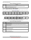
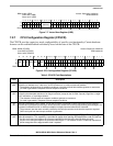
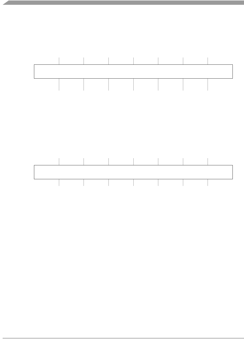
BDM: Load: 0x60 + n; n = 0-7 (Dn)
Store: 0x40 + n; n = 0-7 (Dn)
Access: User read/write
BDM read/write
313029282726252423222120191817161514131211109876543210
R
Data
W
Reset
(D2-D7)
––––––––––––––––––––––––––––––––
Reset
(D0, D1)
See Section 7.3.3.14, “Reset Exception”
Figure 7-2. Data Registers (D0–D7)
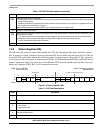
BDM: Load: 0x68 + n; n = 0–6 (An)
Store: 0x48 + n; n = 0–6 (An)
Access: User read/write
BDM read/write
313029282726252423222120191817161514131211109876543210
R
Address
W
Reset––––––––––––––––––––––––––––––––