


Internal Clock Source (S08ICSV3)
MCF51QE128 MCU Series Reference Manual, Rev. 3
254 Freescale Semiconductor
Get the latest version from freescale.com
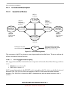
12.4 Functional Description
12.4.1 Operational Modes
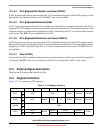
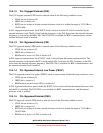
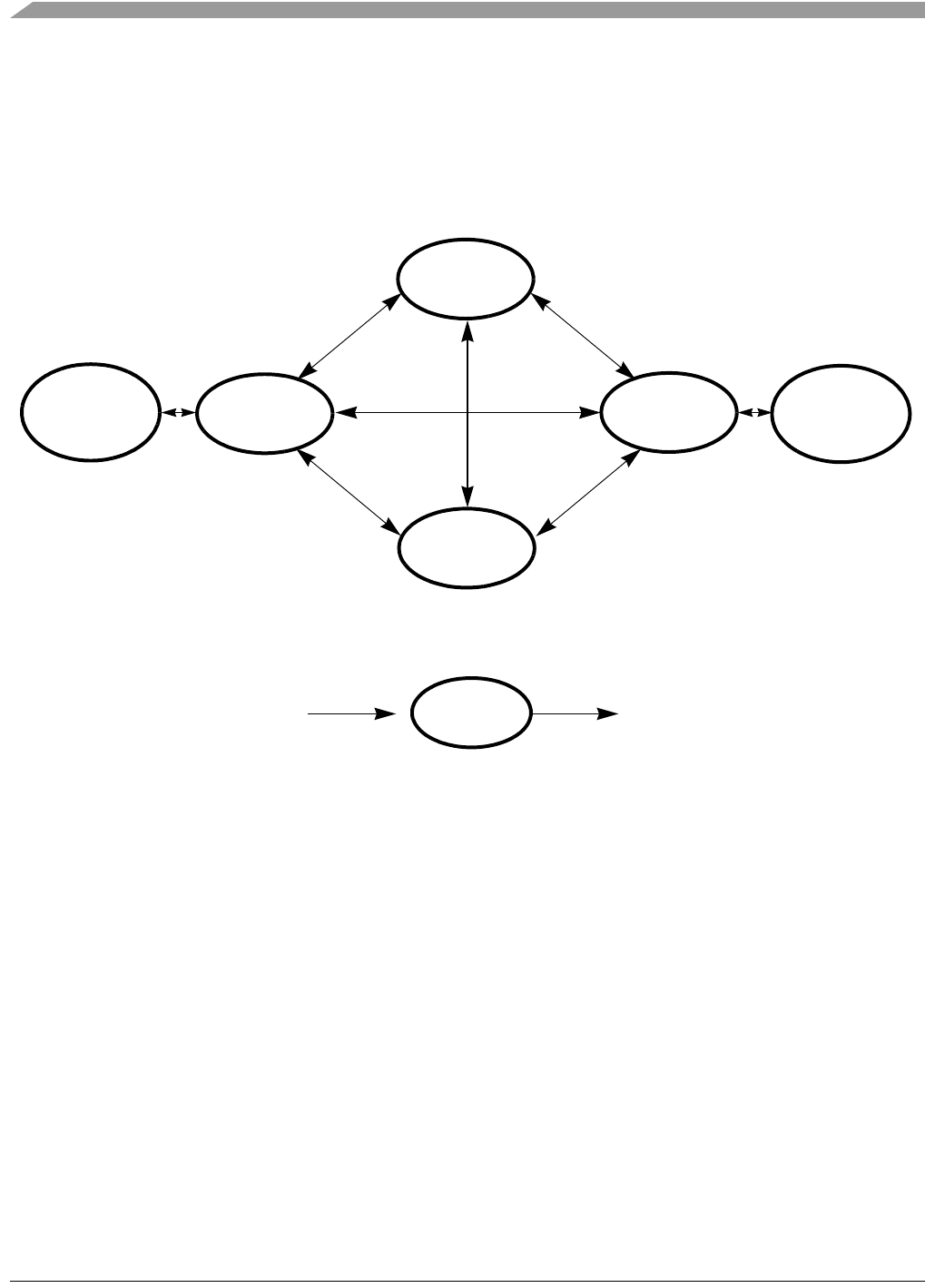
Figure 12-7. Clock Switching Modes
The seven states of the ICS are shown as a state diagram and are described below. The arrows indicate the
allowed movements between the states.
12.4.1.1 FLL Engaged Internal (FEI)
FLL engaged internal (FEI) is the default mode of operation and entered when all the following conditions
occur:
• CLKS bits are written to 00.
• IREFS bit is written to 1.
In FLL engaged internal mode, the ICSOUT clock is derived from the FLL clock controlled by the internal
reference clock. The FLL loop locks the frequency to the FLL factor times the internal reference
frequency. The ICSLCLK is available for BDC communications, and the internal reference clock is
enabled.
FLL Bypassed
Internal Low
Power(FBILP)
IREFS=1
CLKS=00
Entered from any state
when MCU enters stop
FLL Engaged
Internal (FEI)
FLL Bypassed
Internal (FBI)
FLL Bypassed
External (FBE)
FLL Engaged
External (FEE)
FLL Bypassed
External Low
Power(FBELP)
IREFS=0
CLKS=00
IREFS=0
CLKS=10
BDM Enabled
or LP =0
Returns to state that was active
before MCU entered stop, unless
RESET occurs while in stop.
IREFS=0
CLKS=10
BDM Disabled
and LP=1
IREFS=1
CLKS=01
BDM Enabled
or LP=0
IREFS=1
CLKS=01
BDM Disabled
and LP=1
Stop