


MCF51QE128 MCU Series Reference Manual, Rev. 3
Freescale Semiconductor 81
Get the latest version from freescale.com
Chapter 4 Memory
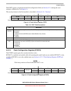
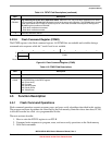
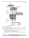
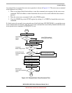
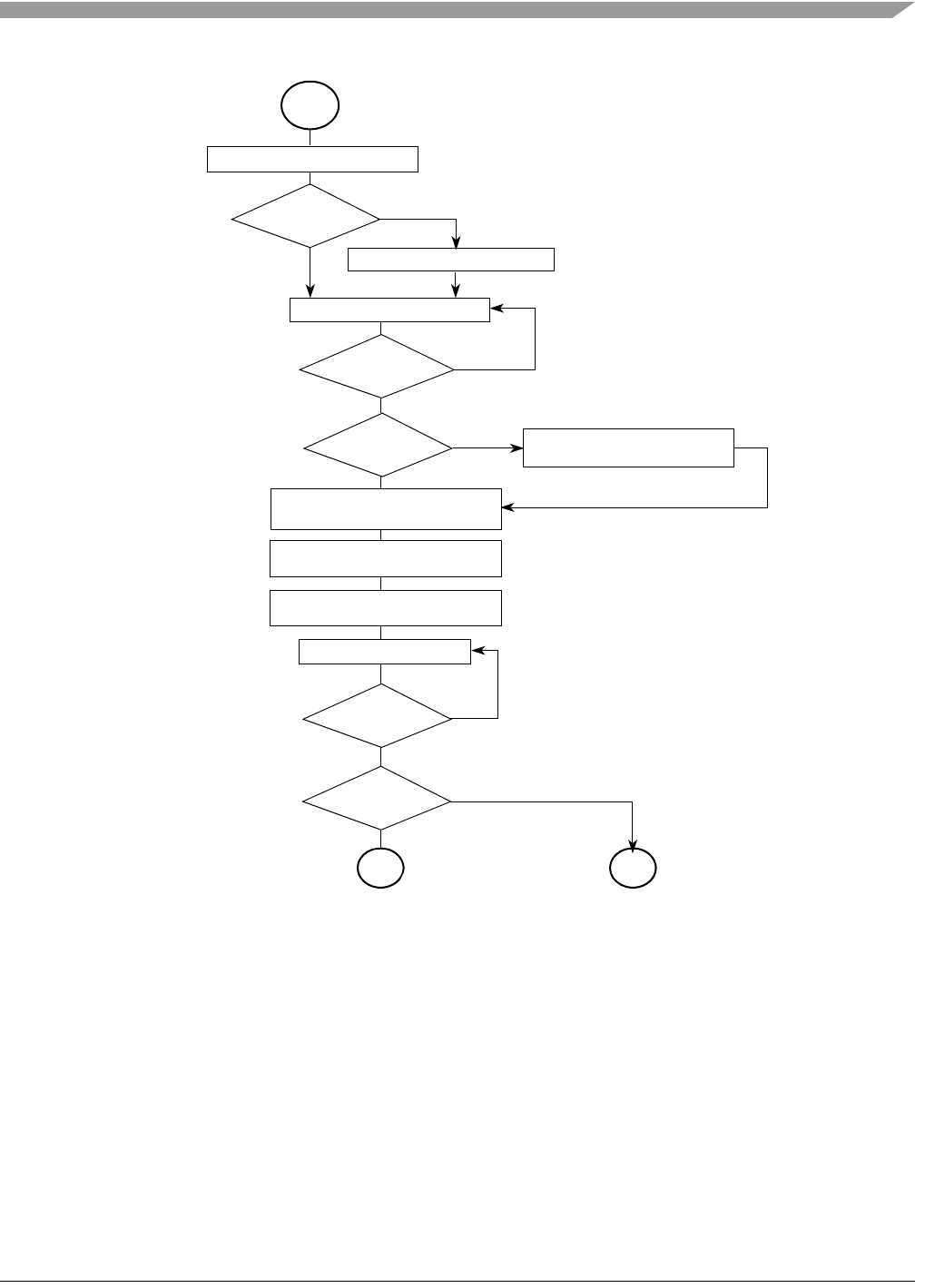
Figure 4-10. Example Erase Verify Command Flow
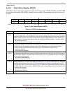
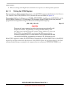
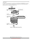
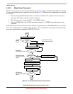
4.5.2.2 Program Command
The program operation programs a previously erased address in the flash memory using an embedded
algorithm. An example flow to execute the program operation is shown in Figure 4-11. The program
command write sequence is as follows:
1. Write to an aligned flash block address to start the command write sequence for the program
command. The data written is programmed to the address written.
2. Write the program command, 0x20, to the FCMD register.
3. Clear the FCBEF flag in the FSTAT register by writing a 1 to FCBEF to launch the program
command.
Write: Flash Block Address
Write: FCMD register
Write: FSTAT register
1.
2.
3.
Write: FSTAT register
yes
no
Access Error and
no
Bit Polling for
Read: FSTAT register
yes
Read: FSTAT register
no
START
yes
FCBEF
Set?
Command
FCCF
Set?
FACCERR/FPVIOL
Set?
no
Erase Verify
yes
EXIT
Flash Block
FBLANK
Set?
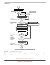
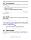
Write: FCDIV register
Read: FCDIV register
yes
no
Clock Register
FDIVLD
Set?
Note: FCDIV needs to
Written
Check
Protection Violation
Check
Buffer Empty Check
and Dummy Data
Erase Verify Command 0x05
Clear FCBEF 0x80
Clear FACCERR/FPVIOL 0x30
Command Completion
Check
Status
Erased
Flash Block
Not Erased
EXIT
be set after each reset